

Biasing a Bipolar Transistor in Common Emitter Configuration
- Boris Poupet
- bpoupet@hotmail.fr
- 7.059 Views
- 0 Comments
- 0 Likes

Presentation of the Common Emitter Amplifier
This article presents how to achieve a proper biasing of bipolar transistors. We take as an example the Common Emitter Amplifier (CEA) as the configuration to study. The CEA is one of the three elementary configurations of bipolar transistors to realize a signal amplifier. A simplified electronic diagram of the CEA with two independent power supplies Vsupply1 and Vsupply2 is given in the following figure :
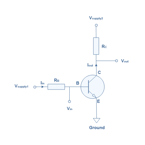
A CEA configuration always presents a resistance linked to the collector where the output current and voltage are extracted.
General characteristics of bipolar transistors
A bipolar transistor has three electrodes represented in Figure 1 by the letters B, C and E, respectively for Base, Collector and Emitter. The base acts like a tap : it controls the flow of electron through the current Iout between the collector and emitter electrodes.
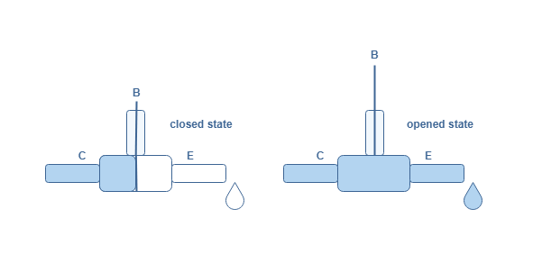
Three different working regions can be distinguished for the bipolar transistors :
- Cutoff region: In this region, the “tap” is closed, thus the emitter, collector and base currents are equal to zero IE=IC=IB=0. The transistor acts as a closed switch.
- Active region: It is the “normal” working region where the “tap” is neither fully closed nor opened. In this region, the transistor’s behavior is linear and the output current is amplified by a base current amplification factor β that is very dependent from the external temperature :

- Saturation region: The “tap” is fully opened. An increase in the base current IB does not affect the output current anymore. The transistor acts as an opened switch.
Biasing of a Common Emitter Transistor Configuration
The name “Common Emitter” comes from the fact that in this configuration, the emitter electrode is linked to the ground and thus the input Vin, Iin and output Vout, Iout are measured between the emitter and the blue dot with the mention Vout represented on Figure 1. First of all, we consider that no AC input signal is delivered to the amplifier, we thus only study the behavior of the CEA in DC mode.
When considering only the base/emitter and collector/emitter, we can clearly establish the following loops :
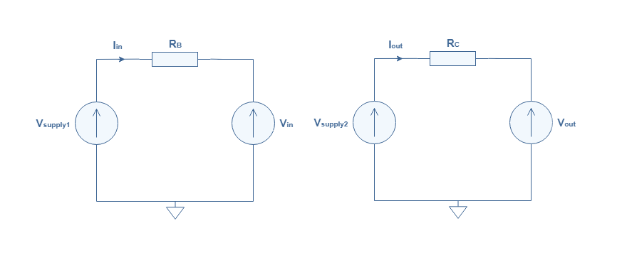
From Figure 3 and using Kirchhoff’s law of potential, we can easily write that :
![]()

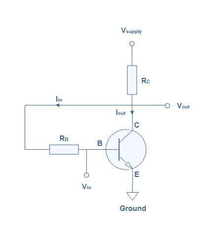
Only one power supply is usually found in CEA amplifiers and delivers a voltage to both the base and the collector so that Equations 1 can be simplified with only one Vsupply. This makes the circuit more simple and decreases the cost.
This process of supplying a DC voltage to the base is commonly known as biasing and is very important to force the transistor to work in his active region.
For the common emitter amplifier, many different biasing methods exist, but some present poor temperature stability : the operating point and parameters of the transistors vary too much with variations of temperature.
The first one, known as the base resistor method is exactly the same as presented in Figure 1 only that the same power supply is shared so that Vsupply1=Vsupply2=Vsupply . In a base resistor biasing architecture, the base resistance RB is very high and chosen such as RB=Vsupply/Iout. This method is very simple to realize since it involves very few components. However, it is rarely employed since the stabilization in temperature of the operating point and the transistor parameters cannot be controlled.
A very small modification of the previous method leads to more stability and is known as the collector to base method.
We can indeed understand without any formula that if Iout increases due to a temperature fluctuation, the voltage across the resistance RC increases so that Vout decreases. The consequence is that the input current Iin decreases, which “closes the tap” and makes the current Iout to decrease. Any variation of the output current is thus controlled by a negative feedback to the input which will counterbalance the fluctuations of Iout.
The most popular and best biasing architecture in terms of stability is the voltage divider biasing method.
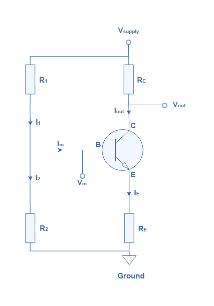
To understand why the stability is improved, a few lines of basic math are required here. First of all, since the input current Iin before amplification is very low, we assume that I1=I2. Considering the voltage loop base-emitter, we can write the voltage V2 across the resistance R2 such as : V2=RE.IE+VBE , with VBE the voltage between the base and emitter of the transistor. When isolating IE and since IE~Iout we can write :

From Equation 2, we can see that Iout is independent from β and thus independent of the transistor parameters and the temperature. The output current Iout is then very stable.
Output Characteristics of the Common Emitter Amplifier
When studying a CEA configuration, one wants to determine how the output Vout is related to the input Vin. One method consists in finding the mathematical expression linking these two values. However, on more complex configurations, this method can be time-consuming and if often leads to mistakes. Another method consists in finding the operating point of the amplifier with its output characteristics and can be measured with proper instrumentation. This method is more visual and easy to realize.
In the following figure 6 are presented the output characteristics (in light blue) Vout, Iout for different inputs Iin,1<Iin,2<Iin,3 as well as the DC load line (in red) defined in Equation 1. For simplification, it is supposed that no particular biasing method is used so that we can refer to the configuration presented in Figure 1 with a single supply voltage Vsupply.
The shape of this figure and the following characteristics on Figures 5 and 6 are not discussed here, their mathematical expression comes from the electronic properties of the semiconductors.
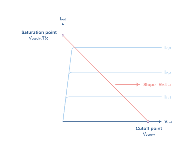
The load line here is given by the formula Vout=Vsupply-RC.Iout and has the mention “DC” because we are under the hypothesis that no swing AC input signal is applied to the amplifier. In order for an amplifier to work, the output voltage Vout needs to match both characteristics of the transistor and the load line. This match is clearly visible on Figure 4 where the load line intersects the blue characteristics of the so called operating points. The input also needs to respect a similar condition as drawn from the example in Figure 5 where the DC load line is given by Vin=Vsupply-RB.Iin.
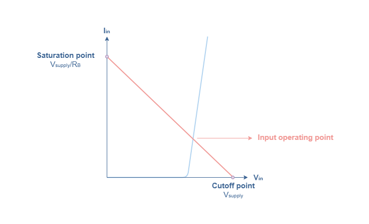
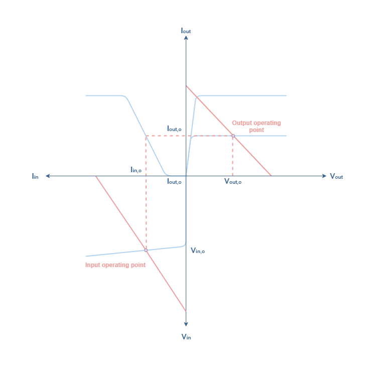
The input, output and DC load characteristics as well as the characteristic Iout=f(Iin) can all be represented in a single graph known as the characteristic network representation. From an input operating point (Vin,o, Iin,o) we can easily determine the output operating point (Vout,o, Iout,o) as shown in Figure 6.
Operating point of a Common Emitter Amplifier
Choosing an appropriate biasing architecture with appropriate resistance values is extremely important to realize a distortion-free amplification commonly called a faithful amplification. In this section, we show graphically throughout the output characteristic curves how important it is to choose an appropriate operating point and biasing method.
Let’s consider a CEA amplifier that accepts an input AC current with a DC value of 10 μA, 20 μA, 30 μA, … and a peak to peak AC value of 40 μA. In the following figures, the operating point is represented as a green dot and the current peak values as purple dots.
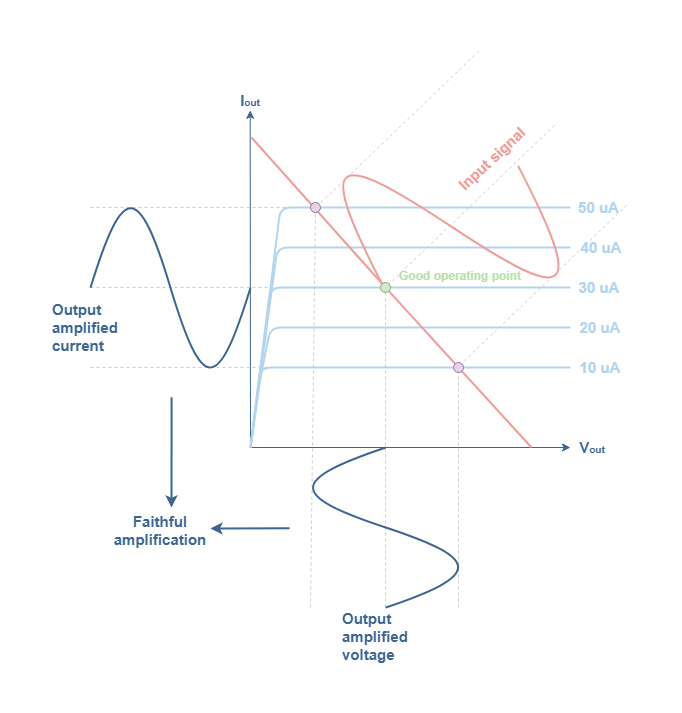
In Figure 7, a representation of a faithful amplification is given. It is shown indeed that the output current and voltage keeps the symmetry of the input signal and are amplified with no distortions. The operating point is thus adapted for an input current with a DC value of 30 μA and a peak to peak value of 40 μA (10 μA to 50 μA).
However, if the biasing architecture is not chosen properly, a distortion of the signal can appear as shown in the following Figure 8.
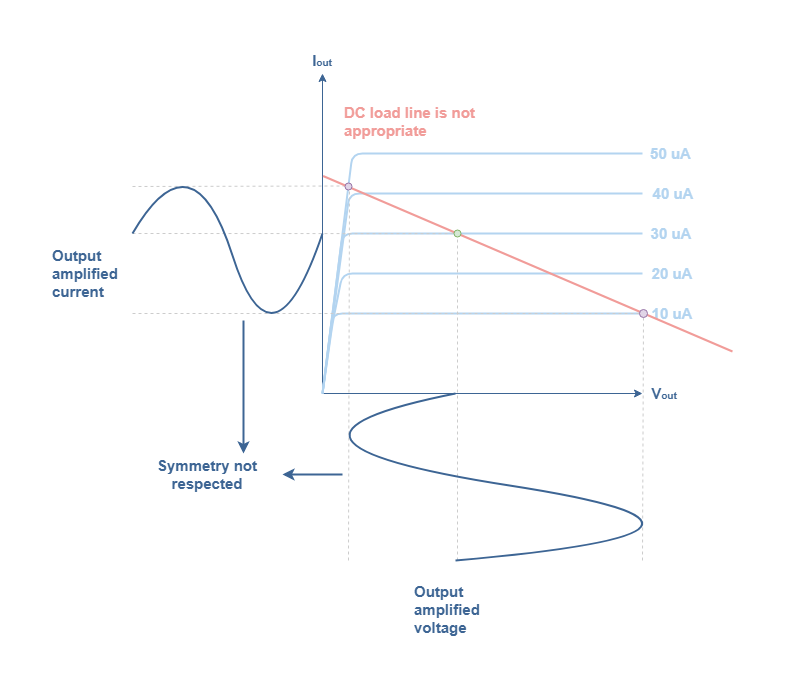
In this example, the DC load line intersects in one point on the 50 μA input curve, the saturation region of the transistor. Since in that region the linearity is not respected, it leads to a distortion of both voltage and current output signals. We can indeed see that the output signals are not symmetrically spread around the mean value (middle grey dashed line).
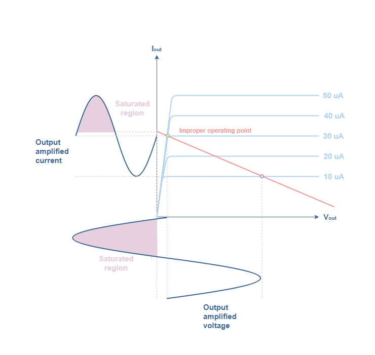
The last example of improper amplification occurs when the operating point is in the saturation region of the transistor. In this case, the output signals are more or less saturated (purple filled region) depending how far the operating is from the active region. The same phenomenon appears symmetrically when the operating point is nearby the cutoff point.
As a conclusion, we have seen through this tutorial how and why to bias a common emitter amplifier. Thanks to the stability it offers, the voltage divider architecture (Figure 5) is the most popular biasing method. By analyzing the characteristics of the CEA configuration and with the concept of operating point, we have seen how an improper biasing can lead to a saturation or distortion of the output signal.
Please follow and like us:
More tutorials in Transistors
Subscribe
Login
0 Comments