

Class D Amplifiers
- Boris Poupet
- bpoupet@hotmail.fr
- 11 min
- 6.677 Views
- 0 Comments
- 0 Likes

Introduction
In the previous tutorials, an important link has been established between the conduction angle of an amplifier and it’s efficiency. Indeed, high conduction angles-based amplifiers offer a very good linearity such as the class A Amplifiers but present a very limited efficiency, generally around 20 to 30 %. As the conduction angle is decreased, high efficiencies are reached such as with the class C amplifiers.
A conduction angle that tends to 0° is therefore desirable to achieve 100 % of efficiency. However, as we have seen with the class C amplifiers, this cannot be implemented since no power is delivered to the load.
Class D amplifiers precisely solve this problem by functioning with a different method than traditional classes A, B, AB or C amplifiers. In the first section, the simplified architecture of a class D amplifiers along with its general functioning are presented. As we will see during this section, class D amplifiers are composed of three different main modules. The next sections are therefore focused on each of these modules to understand how the signal is transformed during the class D amplification process. A little note about the efficiency of this amplifier is given in the last section. Finally, this information is synthesized in a conclusion that summarizes the global transformation of the signal.
Presentation of the Class D amplification
Class D amplifiers generally consists of three different modules : a modulator, a switching stage and a low-pass filter. The signal path along with the succession of these different modules is presented in Figure 1 below :
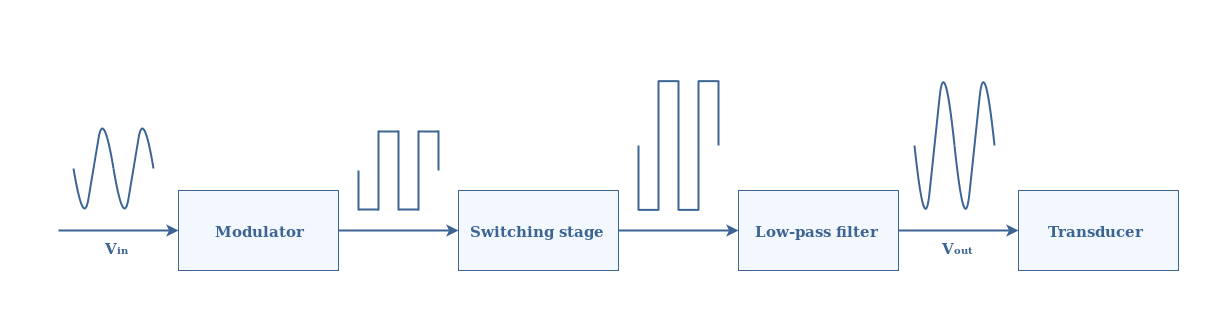
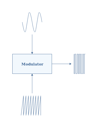
While classic amplifiers accept as an input a sinusoidal signal, Class D amplifiers previously transform it through a modulator into a rectangular signal. We will see in the dedicated section that the view proposed in Figure 1 concerning the modulation is oversimplified.
The switching stage is where the amplification takes places thanks to transistors. We present in detail in the section dealing with this stage that the transistors work in a particular regime and a complementary configuration in order to amplify correctly the rectangle signal.
Finally, a low-pass filter is used in order to restore the sinusoidal shape of the signal. Moreover, this final stage eliminates undesirable harmonics than may have been generated during the amplification process.
Modulation
Many modulations techniques exist, however the most common and widely used for many applications is the Pulse Width Modulation (PWM). A simple graph representing the PWM is shown in Figure 2 below :
This technique consists in comparing the input sinusoidal signal with a high frequency triangular signal commonly called carrier obtained from an independent generator. In order to be consistent with Shannon’s theorem, the frequency of the carrier signal must be at least twice as high as the sinusoidal signal frequency.
The output of the modulator is obtained by doing the following comparison between these two signals :
- If the sine is above the carrier signal, the output is equal to 1
- Otherwise, the output is equal to 0
During the course of this tutorial, the transformation of the signal will be tracked by plotting every step of the amplification with the MatLab® software. In the Figure 3 below, an input signal of frequency 2 Hz is plotted along with a carrier signal of frequency 20 Hz. Moreover, the PWM output is plotted by doing the comparison explained previously.
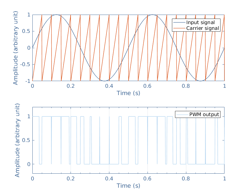
It is important to note that the frequency of the PWM output is the same as the carrier frequency. The duty cycle is the number characterizing the proportion where the signal value is 1 during a period. For example, if the pulse is symmetrical, half of the signal will be 1 and half 0, the duty cycle is therefore 50 % or 0.5. In the case of a PWM, while the frequency is constant, the duty cycle varies.
We can note that when the input signal is maximum, the PWM duty cycle tends to 1 and at the opposite, tends to 0 when the input signal is minimal. Therefore, the duty cycle of the PWM is directly related to the original shape of the sine signal. This affirmation can indeed be confirmed with a simple algorithm that averages the PWM output independently for each cycle, the result is plotted and shown in Figure 4 :
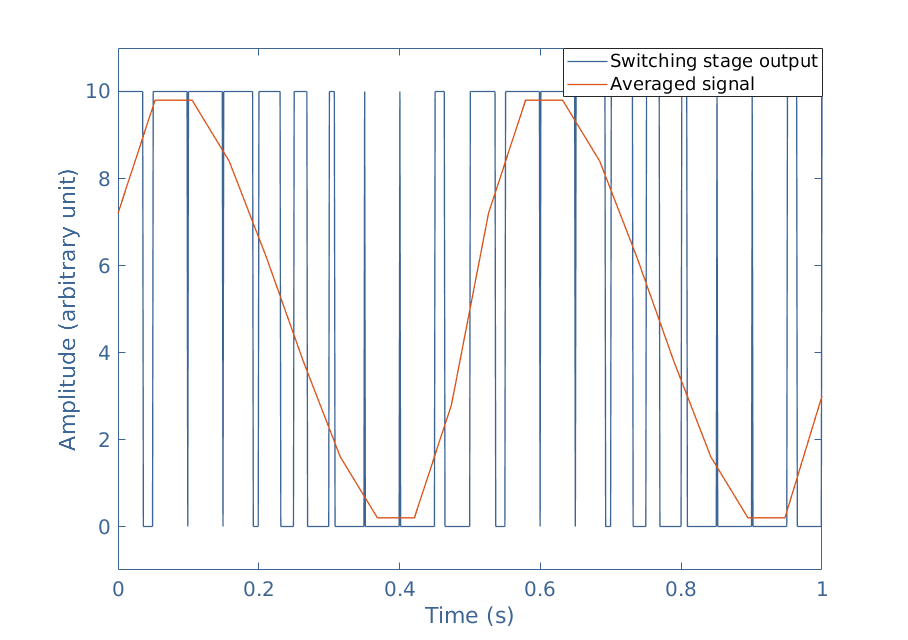
It is clear in this figure that when averaging the PWM signal, the sine shape of the original signal appears again. In real circuits, this operation is done by a filter as we will see in the section “Filtering”.
Amplification
Since the carrier signal is usually chosen such as its frequency is much higher than the input signal, the PWM output to amplify can be above the high cutoff frequency of a BJT-based amplifier (refer to the Frequency Response tutorial). This is the reason why high frequency MOS transistors are preferred over the classical bipolar-based amplifiers for class D amplification.
In a class D amplifiers, one NMOS and one PMOS are connected in a push-pull configuration as shown in Figure 5 :
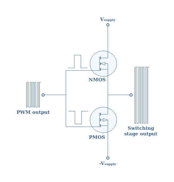
Like for a class B amplifier, the complementary transistors are biased in such a way that the NMOS amplifies only positive half-waves and the PMOS only the negative half-waves. This amplification stage is also called the switching stage because the transistors behave precisely as switches : they are either fully ON (short circuit) or OFF (open circuit).
Filtering
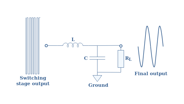
In order to recover the original sine shape of the signal, the amplified pulse signal must be processed by a filter. This filter should respect some conditions :
- Suppress the high frequencies above the normal bandwidth (midrange frequencies) of the amplifier, specially the carrier frequency and its harmonics.
- Reproduce the midrange frequencies of the amplifier with a good level of gain. For example 20 Hz – 20 kHz for an audio amplifier.
- Achieve a maximally flat band for the midrange frequencies.
This kind of filter is commonly known as a Butterworth filter. The typical filter used to fulfill these requirements is a parallel LC circuit. When connected in parallel to a load RL, it actually can be seen as an RLC filter.
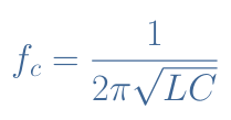
The bandwidth of this filter is characterized by its cutoff frequency fc at -3 dB that satisfies the Equation 1 :
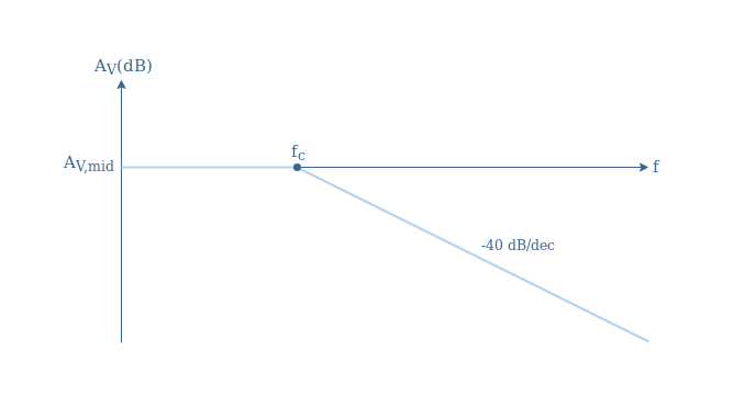
Moreover, since the RLC circuit is a second-order filter, a strong roll-off of -40 dB/dec is observed above fc. An asymptotic diagram of the frequency response of this filter is given is Figure 7 :
Several levels of parallel LC configurations are appreciated since each level increases the order of the filter and therefore the quality of filtration. In Figure 8, we can note the difference between the output resulting of a first or second order Butterworth filter applied to our example :
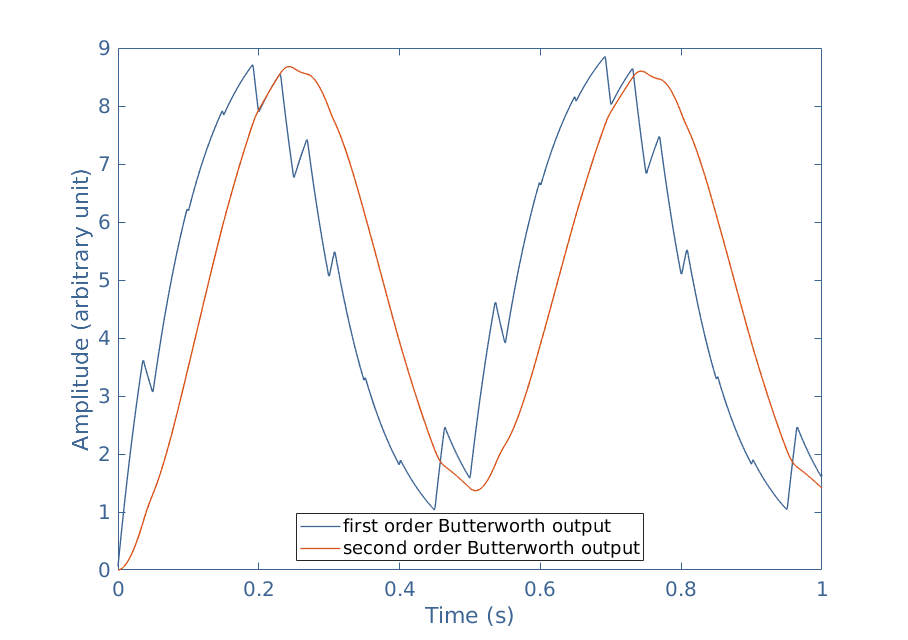
Since the input signal has a frequency of 2 Hz and the carrier frequency is 20 Hz, a cutoff frequency of 4 Hz has been chosen for this filter. We can highlight the fact that a first order filter is not appropriate since it does not attenuate the carrier frequency enough while the second order filter output is much more sinusoidal.
Efficiency
The original way of functioning of the class D amplifier brings its efficiency to very high levels. This high efficiency is explained by the fact that the transistors behave nearly as ideal switches :
- When they are OFF, no current IDS flows between the drain and the source.
- When they are ON, no voltage VDS is observed across the drain and the source.
Therefore, no power VDS×IDS is dissipated in form of losses (heat). Typically the efficiency of class D amplifiers is above 90 %.
Conclusion
Class D amplifiers work very differently than the other typical classes (A,B,C). They are indeed, highly non-linear and incorporate special modules to treat the signals.
The first operation to be done is called a Pulse Width Modulation (PWM) and consists in comparing the input signal with a high frequency triangular signal. Whether the input is above the carrier or under, a new signal called the PWM output is generated and consists of a rectangular signal with the same frequency of the carrier but with a variable duty cycle. This signal is directly related to the original shape of the sine input.
Before getting back a sine signal, a switching stage made with two complementary NMOS and PMOS in a push-pull configuration amplifies the PWM output. The particularity of the transistors is that they switch between being fully ON or OFF, and they never work in their linear zone.
With this amplified pulse signal, a last stage that consists of a L//C circuit that acts as a Butterworth filter to recover the original sine shape. It is important to correctly set the cutoff frequency to eliminate the carrier frequency and its related harmonics. Moreover, a high order Butterworth filter is preferred to avoid as much as possible of distortion.
Finally, we have noted that the efficiency of this amplifier is noticeably higher than the typical classes because of the low power dissipation made possible by the switching behavior of the transistors. This fact is a great advantage in the design of class D amplifier : they do not require heavy and bulky heat sinks.
Due to its many advantages, class D amplifiers can be found in many daily applications : in mobile phones and many audio devices such as earphones, car radios etc …
Please follow and like us:
Subscribe
Login
0 Comments