
Digital Logic Gates Introduction
- Ryan Smith
- ryan@worldofindie.co.uk
- http://www.worldofindie.co.uk
- 12 min
- 1.499 Views
- 0 Comments
- 0 Likes

Introduction
In short, a digital logic gate is a description of a device or circuit that can make a logical decision and has a set of known outputs based on the combination of input signals. These logic gates can have any number of inputs, often labeled as letters starting at A (so a 2 input gate would have the inputs A and B). They also generally have one output, labeled wither Q or Y. These gates can also be combined to make much larger digital circuits, to create a desired function or behavior. These much larger systems can have any number of inputs and outputs and can have either combinational or sequential behavior (we will learn more about the difference later). Logic gates are also not always physical devices. Some devices such as FPGA’s use the logic of logic gates to describe the hardware created within it. Also in software, there are often logic functions that act in the same way but are just a description of the algorithm. Logic gates are all around us and are a key base of computer science.
In this series of tutorials, we will focus on the physical logic chips that are widely available, and a useful resource for engineers starting out. There are two main families of logic chips widely available and accessible, the older CMOS series (Complementary Metal-Oxide-Silicon) which is known as the 4000 series of chips, and TTL (Transistor Transistor Logic) which is the more widely used 7400 series. Note that TTL and CMOS are purely the way the logic is functioned within the chip, and how the chip is fabricated in production. The chips often act in the same logical way, but aspects such as voltages, rise/fall times, and price can all vary between series and manufacturer. There are also other technologies, some older and some newer that produce logic, for instance, RTL (Resistor Transistor Logic) was the technology that ran part of the Saturn V rocket in the 60’s. There is also Diode Transistor Logic and Emitter Coupled Logic. All these components are housed within the chip that is then known as an IC (integrated circuit).
Integrated Circuit Classification
These integrated circuits can often be grouped into different levels of complexity. For instance, a simple XOR gate is much simpler than a modern GPU and has a vast difference in the amount of transistor circuitry involved. There is a common categorization of integrated circuits based on the size that can be used as:
- Small Scale Integration (SSI) containing up to 10 transistors (AND, OR, NOT gates).
- Medium Scale Integration (MSI) containing between 10 and 100 transistors (more complex combinational logic such as Adders, mux, and flip flops).
- Large Scale Integration (LSI) between 100 and 1000 transistors (units using 100’s of logic gates, such as memory, ALU’s and I/O chips).
- Very Large Scale Integration (VLSI) between 1000 and 10000 transistors (small processors, and programmable logic devices).
- Super Large Scale Integration (SLSI) between 10000 and 100000 transistors (microprocessors, microcontrollers, some complex calculators)
- Ultra Large Scale Integration (ULSI) 1,000,000+ transistors (FPGA’s, complex CPU’s, GPU’s and some high end microcontrollers).
There are also devices that go much higher, with devices like SoC’s, which can be as complex as an MPU inside a complex FPGA, and can be known to contain as many as 100 million individual transistors. In 1965 a co-founder of Intel, Gordon Moore came up with what is now known as Moore’s Law, where he predicted that the number of transistors/resistors in a chip will roughly double every 18 months, based on changing technologies. At the time, they were developing technology in the Medium Scale Integration classification, where you would find just over 50 transistors in a chip. The first-ever microprocessor, the 4004, had roughly 2,300 transistors (Large Scale Integration) in 1971. When compared to now, there can be over a billion transistors on a modern Processor.
Logic States
To understand how logic gates work, we first have to understand the rules. Basic digital logic gates perform different functions based on inputs, which we will learn if further tutorials, but they are all based around 2 states. One state is classed as logic HIGH, “1”, or TRUE, and the other state is logic LOW, “0”, or FALSE. Basically, a signal is either ON or OFF. Most of the maths for this was developed by a mathematician called George Boole, who created Boolean Algebra, which you may hear described often in computer science. In Boolean Algebra, you have the states “1” and “0”.
It can be slightly confusing when using some forms of digital logic, as traditionally most logic gates use what is referred to as positive logic, where a positive voltage is equated to a “1” or logic high, but some input/outputs of digital logic-based systems can use negative logic, where a positive voltage is seen as a “0” or logic low. A good example of this is a when an output of something is connected to the cathode of an LED, to turn the LED “ON” you need to set the output to logic “0” or ground. We will discuss this concept further in later tutorials.
Voltage Levels
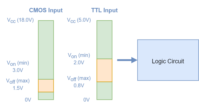
There are many different families of logic gates, and as discussed above, many different technologies get used. Each family within the technology will also have it’s own voltage range that can be accommodated by the inputs to produce that “0” and “1” signal. By in large, TTL is fairly simple with regards to what constitutes a signal. A voltage between 2.0V and 5.0V is a logic high and a voltage between 0V and 0.8V is considered logic low. This is assuming that a +5V rail is used as the power supply, if it is lower, then the upper end of the logic high is reduced to the supply voltage.
Due to the technology of CMOS devices using FET’s rather than bipolar transistors, CMOS uses slightly different logic levels. A logic high is classed as between 3.0V and 18.0V, and a logic low is below 1.5V. Similarly to the TTL voltage levels, the upper limit is reduced with a lower supply voltage. In essence, a logic low should be as close to ground as possible, and a logic high can comfortably be 5V in either technology, with 3.3V operation also being comfortable in TTL based systems. CMOS systems could run on 3.3V, but it would likely be too close to the 3.0V switch, to make a stable circuit.
Digital Noise
Now the digital voltage levels have been clearly defined, we notice there is a clear voltage range in between where a signal can be too high to be “0” but too low to be a “1”. This is useful to stop signals switching erratically during operation, but on occasion, this gap is not actually big enough. This is where noise becomes a real problem, but what is the noise we care about? A signal in a circuit is very rarely a stable voltage, and even if it seems stable, the closer you look, the less stable it appears. Noise is the name given to a random voltage interference on a signal, usually caused by other parts of a circuit, or nearby circuits. Circuits such as power supplies, or fast switching modules can cause electromagnetic radiation, which can cause a spike (where signal goes very high) or a trough (where a signal goes low). If you have an input that is low, and you have a spike, it could read as an input high for a split second, which makes the circuit function incorrectly. There a number of methods that can be adopted including de-bouncing circuits, and Schmitt triggers, but that will be covered in future articles.
The 7400 Family of Devices
As discussed above, the 74 family of logic gates is a very powerful, and widely used TTL bipolar transistor-based family of devices. It is often easy to notice these devices, with it often having a 74 prefix. For instance, a 7400 device is a Quad 2-input NAND gate, and a 7432 is a quad input OR gate. These families go into the hundreds of different circuits, and there are long lists in places such as Wikipedia outlining the general sequence. These devices also come in a number of different sub-families, which define the voltages, speeds and often price of that device. These can be recognized in the letters between the 74 and the device number. Below is a quick list to reference some of the popular subfamilies of 74 logic.
- 74xx or 74Nxx: The standard basic TTL.
- The original devices, introduced in the 70’s.
- Propagation delay of 10ns.
- Power consumption of 10mW.
- Supply voltage range of 4.75V to 5.25V
- 74Lxx: The low power TTL.
- Designed to improve power consumption.
- Slower switching, but less power.
- Supply voltage range of 4.75V to 5.25V
- 74Hxx: The high-speed TTL.
- Designed for faster switching speeds.
- Faster switching, but more power.
- Supply voltage range of 4.75V to 5.25V
- 74Sxx: The Schottky TTL.
- Using Schottky technology.
- Lower impedance, higher switching speed, lower power consumption (~2mW).
- Supply voltage range of 4.75V to 5.25V.
- 74LSxx: The low power Schottky TTL.
- Designed to improve power consumption of Schottky TTL.
- Supply voltage range of 4.75V to 5.25V.
- 74ASxx: The Advanced Schottky TTL.
- Improving the switching of Schottky TTL.
- Much higher switching speeds, but much higher power consumption (~22mW).
- Supply voltage range of 4.5V to 5.5V.
- 74ALSxx: The advanced low power Schottky TTL.
- Improved the previous Schottky TTL devices.
- low power consumption (~1mW), and high switching speeds (4nS).
- Supply voltage range of 4.5V to 5.5V.
- 74HCxx: The High Speed CMOS.
- A very popular form of the 74 family.
- Reduced power consumption, and CMOS compatible inputs.
- Supply voltage range of 4.5V to 5.5V
- 74HCTxx: The High Speed CMOS.
- Designed to reduce power and but lower speed to 16nS.
- Still has TTL inputs.
- Supply voltage range of 4.75V to 5.25V
The 4000 Family of Devices
As with the 74 family of devices, the 4000 series has a common numbering system generally across its families that can be used to remember what they do. They are known for the 40 prefix. CMOS devices can be popular due to their high speed and low power applications, which is why they are employed in some later 74 devices, but the main disadvantage is their susceptibility to ESD (static electricity), also the supply voltage range can be a limitation on occasion rather than a benefit. With modern electronics going to increasingly low voltages to improve switching speeds and power consumption, the 4000 series is seen less and less, and being accumulated into other families. The two common sub-families are:
- 4000B Series: The standard CMOS.
- Original buffered logic, introduced in the 70’s.
- Supply voltage of +3V to +18V.
- 74C Series: 5v CMOS.
- Compatible pinout to the 5V TTL devices.
- Has TTL compatible inputs and outputs.
- Still operate from 3V to 18V.
Conclusion
In conclusion, digital logic gates are highly useful devices that can be used to create much larger circuitry, based on just a few rules. We also learnt about the different physical device families, and some of the implications and considerations needed when choosing the devices to use. This has given us the basis to start learning about the individual logic gates going forward.
Please follow and like us:
Subscribe
Login
0 Comments