Logic AND Gate
- Muhammad Shahid
- m_shahid@live.co.uk
- 1.424 Views
- 0 Comments
- 0 Likes

Logic AND Gate
We know from the Digital Logic Gates Introduction that a digital circuit at its input and output can have only two – states i.e. either “HIGH” or “LOW”. The logic “HIGH” and “LOW” are also termed as “1” and “0” logic, respectively. The voltage level at the input or output is the determinant of the logic “HIGH” or “LOW” and is dependent on the logic family. The Transistor-Transistor Logic (TTL) devices treat 2 to 5 Volts as logic “HIGH” and 0 to 0.8 Volts as logic “LOW”. Whereas, the Complimentary Metal-Oxide-Silicon (CMOS) devices use 3 to 18 Volts as logic “HIGH” and 0.15 Volts as logic “LOW”. The digital logic circuits are commercially available in form of an integrated circuit (IC)/ Chip and may have up to four logic gates inside.
The AND logic returns logic “HIGH” when all of its inputs are in the “HIGH” logic state. In other words, the output of AND gate will be “LOW” when any of the inputs is in the “LOW” logic state. In order to obtain a logic “HIGH”, all of its inputs should be “HIGH” and any of the input turning “LOW” will result in the output being driven to logic “LOW”.
Alternatively, the multiplication of “0”s and “1”s of the inputs gives the output state of AND logic. This gives the Boolean or logic expression of AND logic and is called Logical Multiplication. It is denoted by a dot (.) between the inputs of AND logic gate. For the inputs A and B, the Boolean expression is:
Q = A.B
Resistor-Transistor AND Gate
In the following figure, a basic two-input AND gate constructed using Resistor-Transistor Logic (RTL) are shown. For each input, a Transistor (T) is used and the output is driven across the Resistor (R). In this type of AND logic circuit, the transistors are operated in saturated “ON” & “OFF” states.
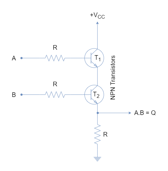
When both inputs “A” and “B” are “HIGH” then both transistors are in saturated “ON” states and a state “HIGH” appears at the output (Q). Turning any of the inputs to logic “LOW” will drive the relative transistor to the “OFF” state and thus incomplete path across VCC & Ground yields state “LOW” at the output (Q).
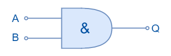
Logic AND Gate Symbol & Truth Tables
The representation of a AND logic by a symbol is shown in the following figure. Its symbol denotes the multiplication/ AND logic operation.
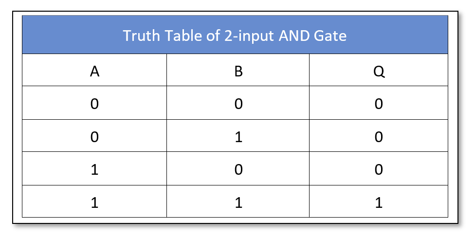
The truth table of a two-input AND logic gate is shown below:
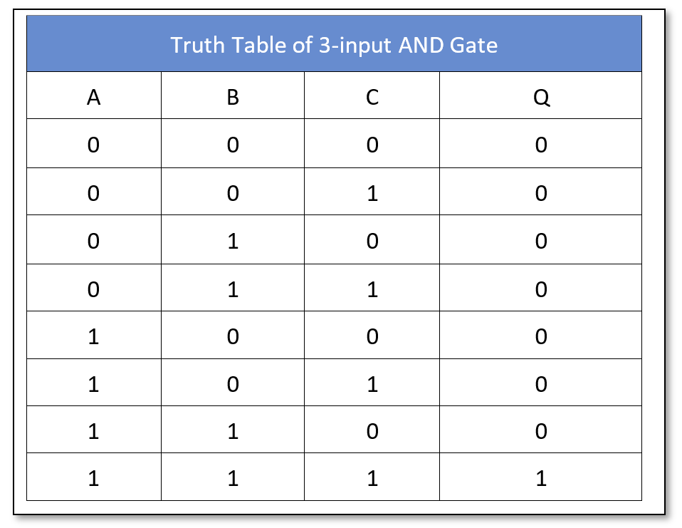
Similarly, the truth table of a three-input AND logic gate is as follow:
The Boolean expression can be extended to include multiple inputs to obtain AND logic operation. However, commercially available AND logic circuits have up to four inputs but the number of inputs can be further extended by cascading the AND logic circuits. In the following figure, three two-inputs gates and one three-input AND logic gate are cascaded to construct a six-inputs (2 x 3 = 6) AND logic circuit.
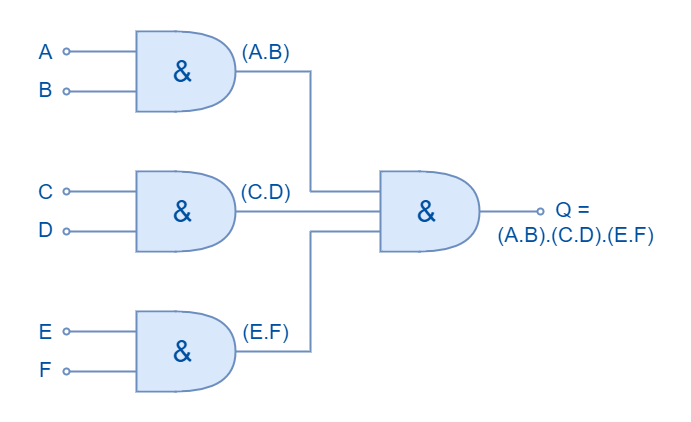
The Boolean expression for this cascaded circuit can be written as:
Q = (A.B).(C.D).(E.F)
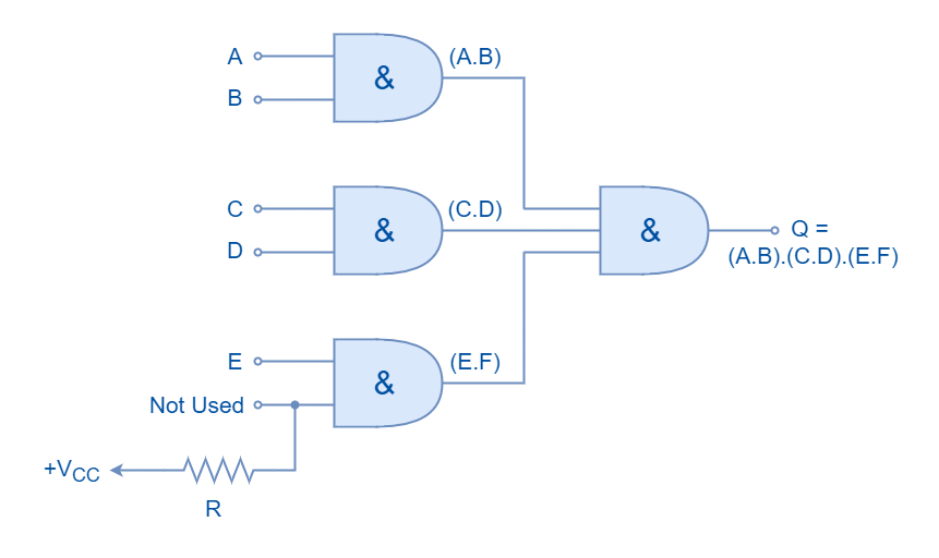
Odd Number of Inputs
The AND logic circuit having an odd number of inputs can be constructed by driving the unused input to logic “HIGH”. This will ensure that another input(s) of the AND logic gate is truly reflected at the output. It is explained in the following diagram where unused input is pulled high using a pull-up resistor.
Commercially Available AND Gates
The AND logic gates are available in both TTL and CMOS logic families. The most commonly used AND logic packages are:
CMOS based AND Gate IC Package
- CD4081 Quad 2-input
- CD4073 Triple 3-input
- CD4082 Dual 4-inputs
TTL based AND Gate IC Package
- 74LS08 Quad 2-input
- 74LS11 Triple 3-input
- 74LS21 Dual 4-input
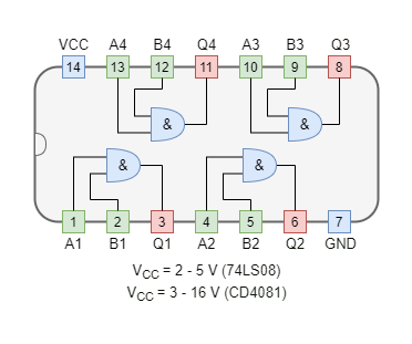
Figure 5: 74LS08 & CD4081 Package having 2-input quad AND gates
Example of AND Logic
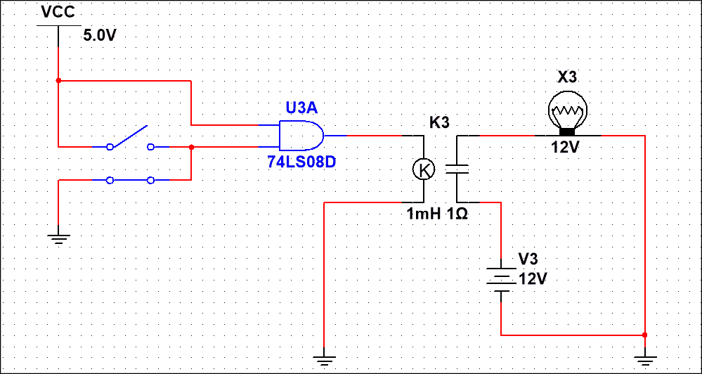
In the following figure, a AND gate is used to drive a 12V relay to switch on the lamp using NI Multisim. The AND gate (74LS08) energizes the relay when all of the inputs are connected to VCC. The relay thus turns on the lamp through an external circuit of 12V. When one of the inputs is connected to ground AND logic goes “OFF” turning the relay and lamp to “OFF” state as well.
Conclusion
- The output of the AND logic is “HIGH” when all of the inputs are in logic “HIGH” states.
- Any of the inputs in the logic “LOW” state will drive AND logic to the “OFF” state.
- The AND logic gates can be constructed using Resistor-Transistor Logic (RTL) but are seldom used because of the propagation delay and power consumption.
- The Transistor-Transistor Logic (TTL) and Complementary Metal-Oxide Semiconductor (CMOS) are commonly used.
- The TTL uses a 5V supply whereas CMOS uses a 3-18V supply.
- The AND logic gates commercially available have up to four AND logic inputs. However, inputs can be extended by using cascaded AND logic gates.
- The AND logic circuit having an odd number of inputs can be constructed by using a pull-up resistor on the unused pin.
- An external circuit can be controlled by AND logic with the use of a magnetic relay.
Please follow and like us:
Subscribe
Login
0 Comments