Logic NOT Gate
- Muhammad Shahid
- m_shahid@live.co.uk
- 1.777 Views
- 0 Comments
- 0 Likes

Logic NOT Gate
The logic NOT gate always returns a not (opposite) of the input signal. It is the simplest and most basic form of a logic gate having only one input and one output. The logic NOT gate is also termed as Inverting Buffer or an Inverter because of its inverting response.
A logic level of “LOW” at the input of a logic NOT gate will be returned as “HIGH” at its output and a logic “HIGH” input will be inverted to “LOW” at the output. In other words, a logic NOT gate complements the input signal at its output.
Because of its complementing response, it is called a logic NOT gate. When the input will be “HIGH” its output will NOT be “HIGH” and, similarly, when its input is “LOW” then its output will NOT be “LOW”.
The logic NOT Boolean expression or logic can be expressed as:
Q= A’
Resistor – Transistor NOT Gate
The logic NOT gate can be constructed using a simple Resistor – Transistor logic as shown in the following figure:
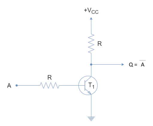
The transistor switches between saturated “ON” and “OFF” states depending upon the signal present at its base. At logic “LOW”, the transistor will be in “OFF” state and the logic “HIGH” appears at the output. Whereas, a logic “HIGH” at the input of the base will switch the transistor to an “ON” state and connects the output to the ground or zero potential. Hence, a logic “LOW” appears at the input. It is obvious that the circuit is performing as a function of inverter or logic NOT gate.
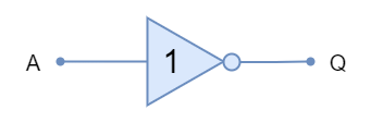
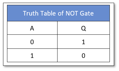
Logic NOT Gate Symbol & Truth Table
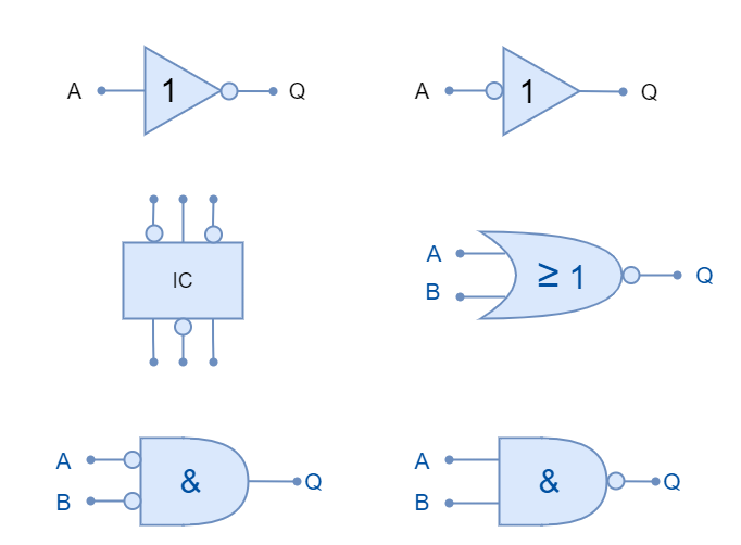
The logic NOT gate symbol has a triangular shape and points towards the output with a circle. The circle denotes the inversion and is called “Inversion Bubble”. The base or flat side of the triangle has the input connected to it. The symbol of a logic NOT gate is shown below:
The simple truth table of a simple NOT gate is:
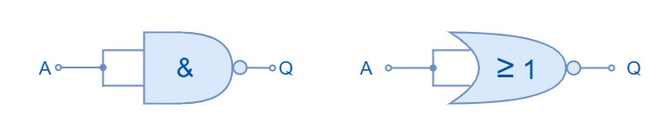
The “Inversion Bubble” is also used in other logic gates to denote the logic inversion. Such as the “Inversion Bubble” at the output of AND and OR gates will represent a logic of NAND and NOR, respectively.
The “Inversion Bubble” can also be used at the inputs to represents an active-low signal which leads to a logic “HIGH” even though the input level is at “LOW”. It is simply an inversion at the input of a logic gate. The active-low signals are represented by circles at the pins of an IC’s pinout diagram.
The following set of figures show a number of variations of logic inversions.
Commercially Available NOT Gates
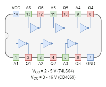
The logic NOT gate is available in both TTL and CMOS logic families. Normally 4 or 6 NOT gates are packed within a single commercial IC package. The most commonly used NOT logic packages are:
CMOS based OR Gate IC Package
- CD4009 Hex Inverter
- CD4069 Hex Inverter
TTL based OR Gate IC Package
- 74LS04 Hex inverter
- 74LS1004 Hex Inverter
Example of OR Logic
In the following figure, a NOT gate is used to drive a 12V relay to switch on the lamp using NI Multisim. The NOT gate (74LS04) energizes the relay when a “LOW” logic input is applied. The relay thus turns on the lamp through an external circuit of 12V. When the input is at the logic “HIGH” level, the 74LS04 will invert the “HIGH” to “LOW” and switch off the relay to turn off the lamp.
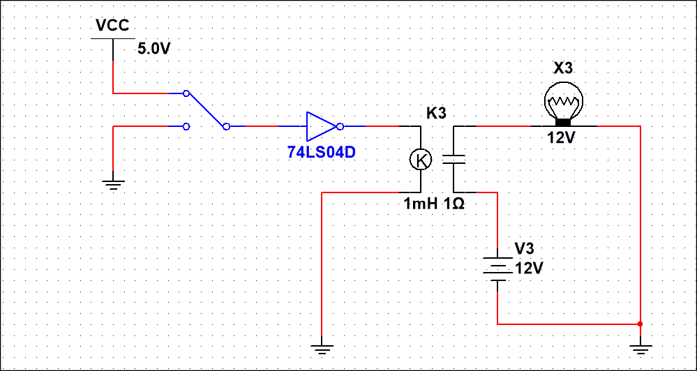
Figure 5: A Multisim circuit showing “NOT” logic to control an external circuit
NAND and NOR Gate Equivalents
An inversion logic or NOT logic can also be achieved by using NAND or NOR gate. A simple 2-input NAND or NOR gate can be used for this purpose as shown below figure. The inputs of NAND or NOR gate are shorted to make a common input and outputs of NAND and NOR gates are dependent on this common input which will always be inverted.
Schmitt Inverter/ Hex Inverter
As discussed above, a logic NOT gate can be constructed using a transistor. However, transistors take time to switch between saturated “OFF” & “ON” states. The switching is accompanied by some time delay in transistors and is not instant. Moreover, the transistor has the dominant characteristic of amplification and which may lead to its operation in amplification mode. In linear amplification operation, a small change in the input leads to a significant change in its output which can also cause to switch between “OFF” & “ON” states abruptly. A Schmitt Inverter or Hex Inverter can be used to avoid these problems.
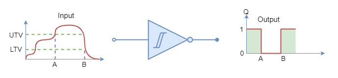
As discussed in the previous article(s), in TTL family 2 to 5V is considered as logic “HIGH” and 0 to 0.8V as logic “LOW”. The voltage level of 0.8 and 2V can be set as Lower Threshold Voltage (LTV) and Upper Threshold Voltage (UTV), respectively. The Schmitt Inverter operates on these LTV and UTV limits and changes its state instantly. Whenever the input voltage level rises above UTV i.e. 2V then Schmitt Inverter output changes to logic “LOW” (obviously, it is an inverter), and as soon as input voltage drops below LTV i.e. 0.8V then its output changes to logic “HIGH”. It keeps the previous state during the transition period and switches state instantly upon reaching threshold voltages. It can be said to have a Hysteresis built into the Schmitt Inverter.
Schmitt NOT Gate Oscillator
A very useful and common application of Schmitt Inverters is found in oscillators.
Square-Wave Oscillator
A simple Schmitt RC oscillator is shown in the following figure.
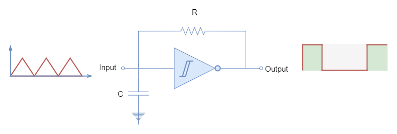
Initially, the capacitor is discharged and zero voltage is present at the input of Schmitt Inverter which is equivalent to logic “LOW”. Resultantly, a logic level of “HIGH” appears at the output due to inversion and the capacitor starts charging through the feedback resistor (R). The Schmitt Inverter changes its output from “HIGH” to “LOW” as soon as the capacitor charges to the upper threshold limit (UTL). The capacitor then starts to discharge through the feedback resistor (R) and Schmitt Inverter changes state from “LOW” to “HIGH” as soon as capacitor voltage hits lower threshold limit (LTV). The switching of the states continues producing a square wave at the output.
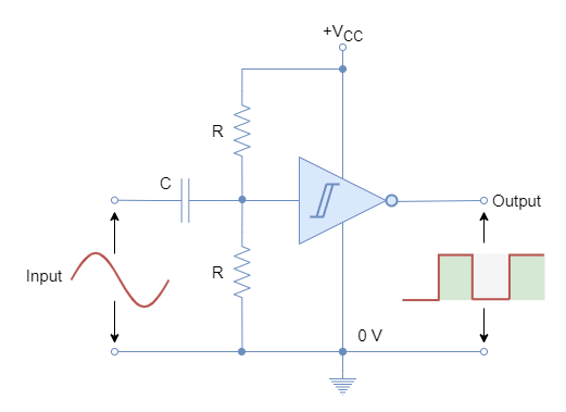
Sine-to-Square Wave Converter
The following Schmitt Inverter circuit converts the Sine-Wave to a Square-Wave. The voltage divider at the input of the Schmitt Inverter sets the quiescent point. Whereas, the capacitor at the input acts as a decoupling capacitor to block the DC component and allows Sine-Wave to pass through it. The Sine-Wave magnitude passes through UTV & LTV of Schmitt Inverter and the output of Schmitt Inverter switches between “ON” and “OFF” states. A Square-Wave appears at the output having a switching frequency equal to that of the Sine-Wave.
Conclusion
- The NOT gate has a logic of inverter and an inverted logic of input appears at the output.
- A logic NOT gate results in a logic “LOW” when input logic is “HIGH” and in a logic “HIGH” when input logic is “LOW”.
- The NOT Gate is also called an Inverter Buffer or simply Inverter.
- It is symbolized by a triangle with a circle at its output terminal. The circle is termed as “Inversion Bubble” and is commonly used at the terminals to denote an inversion or active-low input.
- The logic NOT can also be achieved by using NAND or NOR gate.
- The logic NOT can be constructed using Resistor – Transistor Logic but TTL, CMOS & Schmitt Inverters have logic NOT gates commercially available in IC packages.
- The Schmitt Inverter or Hex Inverter overcomes the issues of switching delays due to transistors-based logic circuits.
- The Schmitt Inverters are commonly used in oscillators and signal converters.
Please follow and like us:
Subscribe
Login
0 Comments