

OPAMP Integrator
- Boris Poupet
- bpoupet@hotmail.fr
- 13 min
- 15.337 Views
- 1 Comments
- 1 Likes

Introduction
In most of our previous tutorials related to operational amplifiers, the configurations were based on amplifiers with resistors as part of the feedback loop, voltage dividers, or to interconnect many op-amps. This new tutorial presents a configuration called integrator in which a reactive component (capacitor) is added in the design.
In the first section, we will focus on the functioning of the integrator by showing how the capacitor affects the circuit and the AC response of the circuit is also presented. Moreover, we demonstrate its output voltage formula and highlight why this circuit can be labeled as an integrator.
The basic configuration presented in the first section presents limitations that are exhibited in the second section. “Real” or “Practical” integrator circuits are presented and we investigate how similar they are with their ideal equivalent.
Presentation
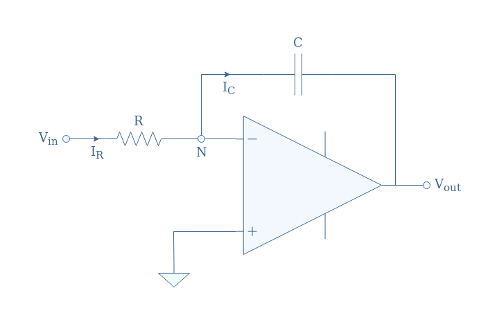
Functioning
An integrator consists of an inverting op-amp in which the resistor present in the feedback loop is replaced by a capacitor. The basic design on an integrator is presented in Figure 1 below, we will also refer to this circuit as the ideal integrator.
The behavior of the integrator is mainly dictated by the electric behavior of the capacitor. We remind in particular the constitutive equation of the capacitor:
With VC being the voltage across the capacitor, C its capacitance, and Q its charge.
From Equation 1, we can understand that a capacitor reacts to variations of voltage. Indeed, if no variation is happening, no current is observed but if the voltage across the capacitor varies, it discharges and lets the current pass.
In other words, in DC regime, a capacitor is equivalent to an open circuit while in the high-frequency regime it tends to be a short circuit as the frequency increases.
When we apply this observation in the context of the operational amplifier, we can see that in the DC regime the circuit of Figure 1 is equivalent to an op-amp in open-loop configuration (non-linear regime) and behaves therefore as a comparator.
However, when variations of the input are present, the circuit tends to be equivalent to an inverting buffer op-amp (refer to the tutorial Op-amp building blocks) as a negative feedback loop is established:
Keeping this behavior in mind, it is interesting to focus on how the integrator circuit reacts to a Heaviside input, which is also known as the step response:
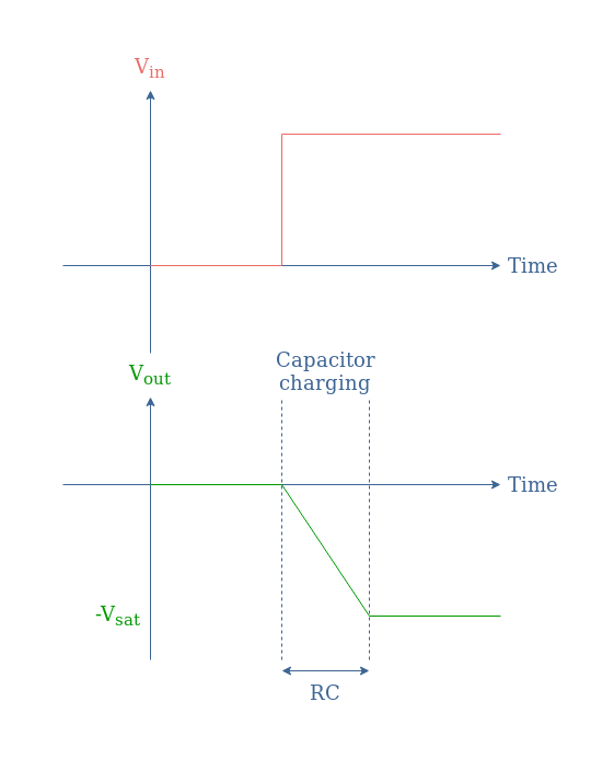
It is interesting to note that the saturation voltage Vsat limits the integration operation since the negative ramp of Vout should continue as long as Vin≠0.
AC response
The most important fact to keep in mind from Figure 3 is that a time limitation given by the value R×C exists for the amplifier to switch from one state to the other. In other words, as the frequency increases, and the circuit tends to behave more like a voltage follower, the harder it will be for the op-amp to actually “keep-up”.
We can illustrate this phenomenon with the following Figure 4 showing the output of the integrator when a square signal of period T is applied at its input.
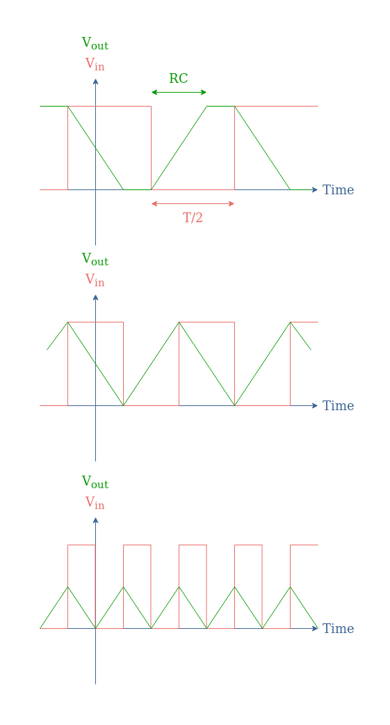
In the first case, T/2>RC which makes the output to saturate for a while. In the second case, T/2≅RC is the regime where the integrator performs well the integration operation. Finally, when T/2<RC we can see that the integrator cannot efficiently follow the speed rate.
In order to really understand the behavior of the ideal integrator regarding the frequency, we can apply Millman’s theorem to the node N (Figure 1), which gives:
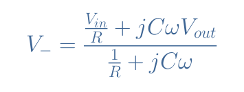
If we suppose the input impedance of the op-amp to be infinite (which is not true but a good approximation), V–=0, and therefore:
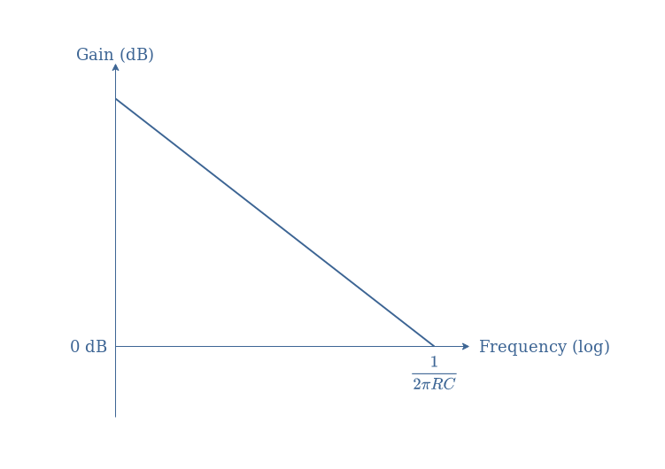
With T being the transfer function of the circuit and x=ω/ω0 (ω0=1/RC). If we convert this data in dB, the gain of the ideal integrator is given by -20log(x), which is a decreasing linear plot G=f(log(x)). The signal phase φ(ω) is here constant and given by the argument of T, since arg(T)=arg(-1)-arg(jx), φ=π-π/2=+π/2.
As a consequence, the Bode diagram of an ideal integrator is given by the following Figure 5:
Output formula
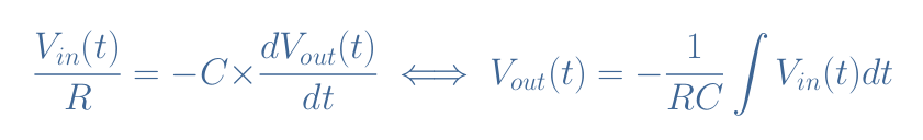
If we suppose the op-amp in Figure 1 to be ideal, the hypothesis i+=i–=0 and V+=V–=0 are verified due to its infinite input impedance. Therefore, the current across the resistor IR is equal to the current across the capacitor IC.
This current can simply be expressed by I(t)=Vin(t)/R when applying Ohm’s law to the input branch, moreover, we can apply Equation 1 in the feedback loop to write a second expression of the same current: I(t)=-C×(dVout(t)/dt).
Finally, when equalizing the two expressions of I(t), we get the output formula of the integrator op-amp shown in Equation 3. This formula highlights the fact that the output is proportional to the integral of the input signal.
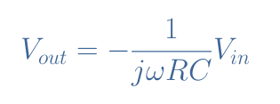
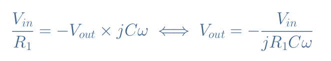
Equation 3 can actually be simplified by using the complex notation:
Limitations
As we highlighted in the previous section, the circuit presented in Figure 1 presents the inconvenience of behaving like a comparator when a DC input is applied to it. This could not be a problem if the amplifiers are considered ideal supplied with signals without any DC component such as pure sine waveforms for example.
However, in real circuits, op-amps always present an off-set voltage (refer to the corresponding tutorial) which would make the configuration in Figure 1 always saturate, even without any input signal.
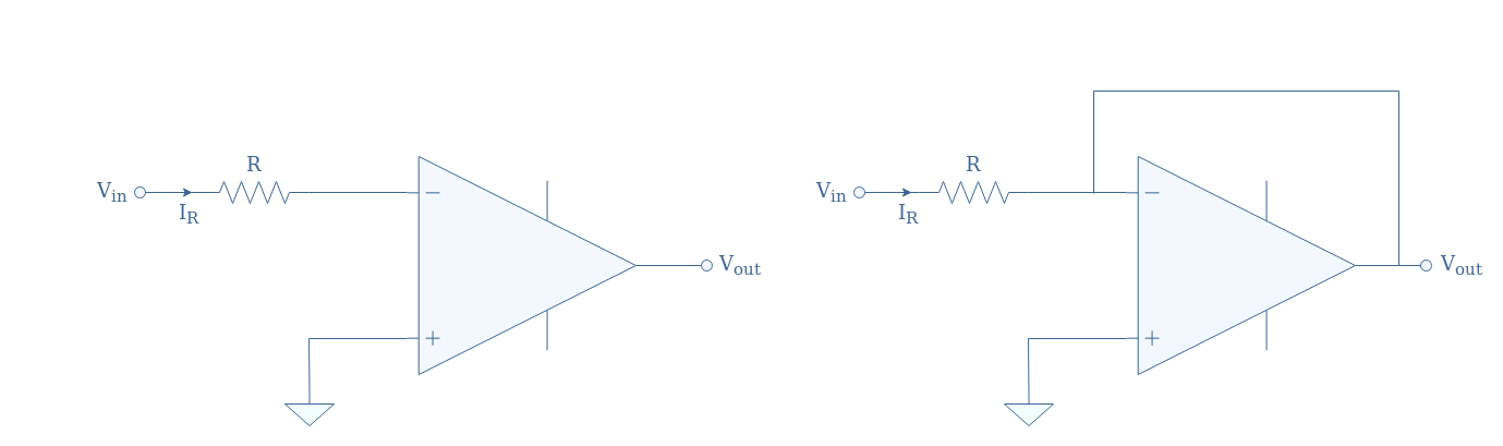
In order to solve this undesirable behavior, a resistor can be added in parallel with the capacitor to obtain the so-called pseudo-integrator circuit:
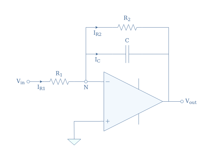
In the DC regime, when the capacitor C acts as an open circuit, the resistor R2 provides a feedback path allowing the circuit to behave as an inverting amplifier with a closed-loop gain -R2/R1.
At high frequencies, the capacitor shortens the resistor R2 making the circuit tend to behave as an inverting voltage buffer.
So why is this circuit called a “pseudo-integrator”? In order to answer that question, let’s again apply Millman’s theorem to node N in Figure 6:
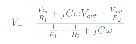
Due to the same hypothesis as previously mentioned, V–=0, which leads to the expression of the transfer function of the real integrator:
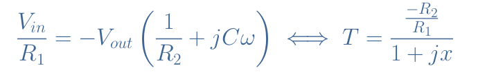
The parameter “x” is here given by ω/ω0 with ω0=1/R2C playing the role of the cutoff frequency at -3 dB. For frequencies from DC up to ω0, T can be approximated to -R2/R1, hence the gain being given by 20log(R2/R1). At ω0 and above, the gain experiences a -20 dB/decade loss, similarly to the ideal integrator, the gain is equal to 0 dB for ω=1/R1C.
As for the phase of the signal, it varies from π when the gain is constant to π/2 when the frequency tends to infinite values.
With this information, the asymptotic Bode plot of the real integrator can be given in Figure 7:
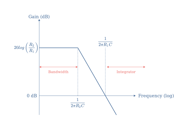
As a consequence, we can say that a real integrator behaves as a low pass filter with a cutoff frequency depending on the capacitor and resistor present in the feedback loop.
From the first part of Equation 4, we can see that when the frequency is very high, the equality between Vin and Vout is reduced to:
This equation is similar to the ideal integrator transfer function given by Equation 4 pseudo-integrator circuit and we can conclude that the real integrator circuit is a good approximation of an ideal integrator for frequencies significantly higher than its cutoff frequency.
Conclusion
The mathematical operation “integration” can be realized by an electronic circuit called an integrator, which is based on an operational amplifier working in inverting configuration with a reactive component in its feedback loop.
We highlight in the first section how the frequency behavior of the capacitor modifies the entire functioning of the circuit by alternatively opening and closing the feedback loop when variations of the input signal are present.
Due to the charging and discharging time of the capacitor, we show that depending on the frequency of the input signal, the circuit follows more or less the variations. When the frequency is too low, the output tends to reach the saturation level which is not part of the integration operation. On the other hand, when the frequency increases too much, the gain of the output drastically decreases by 20 dB/decade.
The ideal circuit presented in the first section cannot practically be designed due to its tendency to saturate any DC component present in the input signal. To solve this behavior, an extra parallel resistor is added in the feedback loop for real integrators. As a consequence, the circuit acts as a low-pass filter and start to properly integrate the signal only above a certain frequency given by the product of the capacitor and resistance in the input branch.
Please follow and like us:


I imagine that the op influences the frequency response of the integrator circuit. But in what way? That is, we choose the appropriate values of R1, R2 and C so that the circuit integrates in the range of frequencies that we are interested in. So, how do we determine the properties that the operational must have (bandwidth…)?
Thanks!