

mixos
-
Posts
581 -
Joined
-
Last visited
Content Type
Profiles
Forums
Events
Posts posted by mixos
-
-
Hello
OA47 is a Germanium Gold Bonded Diode. It's an old fashion diode and it isn't used in our days. You can try a 1N34, 1N34A, 1N64, 1N64A, 1N914 instead.
About your first question i am not able to answer you. -
The best way to hanlde electrostaticly sensitive devices is to supply your work bench with an antistatic mat which is connected to the ground. Also you must discharge yourself. For that reason use a conductive wrist connected to ground. There are special Antistatic Work Surface Kits and equipment like below:

But in case you what to handle electrostatic sensitive devices occasionaly and don't want to buy any special equipment, follow the rules below :
1. Don't handle CMOS circuits directly.
2. Avoid touching metal leads and other circuit areas when handling devices with CMOS parts.
3. Discharge your hands by touching a fount.
4. Try to handle CMOS from it's case.
5. Use a pincer to install the cmos, which you have connected to the ground.
If you follow these rules you can install it succesfully. Keep in mind that cmos can be installed succesfully without following any of these rules if you are lucky, but these rules will reduce the chance to damage it. -
Hello EDY!
You are right, the english writing of a japanise people reflects the japanese complexity !!
hFE is a number which accompany each BJT transistor (may differ from transistor to transistor). It's a number that tells you how many times the base current will be multiplied and finally ampified. The amplified current it's the current that flows from C (collector). You need to know this if you are using the transistor for amplification. If you use it just for a on-off state you don't care much about it.
You must believe (like a principle) that the BE voltage when transistor conducts is 0,6V. It's like the constant voltage of a common diode right polarized. Also a voltage of about 0,2V exists at CE when the transistor conducts.
Having this things in mind (also the 12V at IN) you can easily calculate the resistor current. The base current must be enough to take the transistor in full conduct. It is controlled by R1. So R1 must have such a value to make the transistor condust. If the base current is small then the C current is proportional to this small current. If the base current exceed a value (it depends on the transistor) then the C current depends on the internal resistance of the relay because it like closing a switch between Collector and Emitter.
I wish i helped to clarify the transistor characteristics, but keep in mind that it's not so easy to understund the BJT transistor in one day. Everyday you will detect a new characteristic until you finally undestand it completely.
Tell me if something went wrong. -
I found this Frequency Multiplier:
http://users.otenet.gr/~athsam/frequency_multiplier.htm
I think it's exellent for your case. With it you can multiply a frequency of 1Hz (or below) a hundrent times.
Which is the minimun frequency that LM2917/LM2907 can be driven? -
-
Yes you can post almost everything. I will add it if it is helpfull. You can send it via e-mail also, until the Action Section is online.
-
Hello
I am planning to add the abbility to let users upload (and then publish) their circuits. The credits will be all theirs.
Have you got another idea? Drop it here.. -
Hello EDY
I attach you the datasheet of bzx85c diodes series. It's only 58,8kB
Tip: when you search for a part's datasheet like the above bzx85c180, try to guess if there is a main name and a prefix of subfix, like happened in this situation. The bzx85c is the diode number and the 180 is the subfix.
With a search string bzx85c180 you will not find any datasheet, but with bzx85c.pdf you will find some.
Cheers ;) -
If you look at the pinout of each circuit you will notice that they are the same. Also the internal circuit it's the same.

-
1. Right! CD4027 is a CMOS Dual J-K Master-Slave Flip-Flop with Set-Reset capability
2. Datasheet download: cd4027b.pdf (408 kb)
3. Pin 1 & 2 are not used.
4. Yes -
The best program you can use is GSview
The home page is: http://www.cs.wisc.edu/~ghost/
The download page is: http://www.cs.wisc.edu/~ghost/gsview/get44.htm
Or download directly form here:
gsv44w32.exe Win32 self extracting archive
gsv44os2.zip OS/2 archive
gsview-4.4-1.i386.rpm Linux RPM
gsview-4.4.i386.tar.gz Linux executable
gsv44src.zip Source archive
Also it can reads PDF files!
Hope that helps ;) -
The good think is that there is a special Silver Conductive Pen and with it you can make conductive traces to design a circuit. Mainly it is used to repair pcb faults.
The bad thing is that you must route the circuit by hand and maybe you must use a transparency paper or another paper of same surface to avoid absorbe into it.
I don't know if there is a special ink for your printer to make your life easier but i think it's improbable in common inject printers to do that even if the ink exists.
Take a look:

Also visit some manufactures:
http://www.mgchemicals.com/products/8420p.html
http://www.intertronics.co.uk/products/tec2505.htm -
By clicking here you can download a circuit that is an ion generator and consists of a voltage multiplier circuit.
This is a usage of an voltage multiplier circuit :)
Also this is another design of the voltage multiplier:
-
You can use a switch of this type if it is suitable:
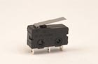
I can't find something closer to a mercury switch. You can also attach a bob on top of the foil to make it more motion sensitive. -
Hello

You can also check the following site for more photos - info:
http://www.geocities.com/SunsetStrip/Underground/8585/loop.html
http://www.iri.tudelft.nl/~geurink/magnloop.htm
http://www.uksmg.org/loop.htm
http://www.standpipe.com/w2bri/
http://www.radioworks.com/nloop.html
http://www.g3ycc.karoo.net/loop.htm -
This happens if you measure the voltage across the final diode.
If you measure the voltage at the point where the last capacitor and diode are connected (upper right corner of the circuit) refering to the ground then the voltage you measure is the multiplied one. -
Here is a list of speaker designing sites ;) :
Audio Illusions: http://indigo.ie/~walton/audio1.html
The 3D-Spiral Horn Speaker Building: http://www3.ocn.ne.jp/~hanbei/eng-intro.html
Audio Lab Loudspeaker Plans : http://www.ee.gatech.edu/users/207/labsp/
Audio Lab Loudspeaker Plans (2) : http://www.ee.gatech.edu/users/207/labsp2/
William Cowan's Peerless 831857 subwoofers : http://www.geocities.com/ResearchTriangle/9329/tlees.html
The Russ Button Subwoofer : http://www.button.com/Russ/audio.shtml#subwoofer
Monolith Subwoofer (Jerry Lynds) : http://husky1.stmarys.ca/~j_lynds/Monolith.htm
Paul Horn's Subwoofer (6th order) : http://www.linkline.com/personal/phorn/audio/hs_subwoofers.html
Luther Ward's Sub Atomic Express : http://wardsweb.org/audio/beast.html
Patman's SUNosub : http://www.io.com/~patman/sunosub.html
S -
After a little research i noticed that the semiconductors packages are millions!! :o. Also each company has it's own.
Some common packages can be found here:
http://www.necel.com/discrete/english/products/transistor/pkgquick.html -
Here is a list with high power fm transmitter circuits 8) :
http://www.see.ed.ac.uk/~gjrp/EE3/Comms/Lecture10/sld009.htm
http://www.aaroncake.net/circuits/3Wfmtran.htm
http://members.tripod.com/xexorz/schematics/fmtrans1.html
http://w1.859.telia.com/~u85920178/tx/v6_00.htm
http://w1.859.telia.com/~u85920178/tx/v7b_proj.htm
http://www.radio101.de/radio101/schalt-e.htm
http://www.geocities.com/Area51/Nebula/3736/40watt.html
http://w1.859.telia.com/~u85920178/tx/bug5.htm -
The best way is to use a FM Linear like this:
Linear FM 30Watt : http://www.electronics-lab.com/projects/rf/010/index.html
This circuit connects to the output of your transmiter and it is able to make a 4-5W transmitter to 25-30W one.
Alternative you can use a FM antenna booster (active antenna) like this: http://www.electronics-lab.com/projects/rf/022/index.html
About the anntenas you can read this article: http://www.scott-inc.com/html/fmant.htm -
The designer of the circuit writes that the filter must be driven by a preaplifier, but i think that it can be also driven by an amplifier directly.
Don't worry about the pontesiometers. They will do the jod.
I haven't tested it, so i don't know about any effect in the cut-off frequency.
No there is no need of a crossover. The circuit will cut off all frequences out from the 20-100Hz ragne. -
A list of Heathkit transistors can be found here:
http://www.sarrio.com/sarrio/rsman2.html
I wish this helps you. ;)
Mike -
Did you mean BPW77 Transistor ?

BPW77N is a very high sensitive silicon NPN epitaxial planar phototransistor in a standard TO -
I use OrCAD which is a compete electronics development studio. It includes schematic capture, spice and layout editor.
I like it but it is not very easy to design a pcb. It has autoroute function but it is not so "clever" it can turn a simple pcb into a huge one. Maybe i make a mistake in operetion of that software.
Otherwise you can use it to manual route your pcb and then the result can be nice.
The component database is huge also and i have not noticed any pad problems.


Transistor tester
in Projects Q/A
Posted
mozikluv you and your questions are always welcome :) !
1. Attach the plier to the ground for some seconds to discharge it. Handle it from an insulated grasp. Then align the pins without fear. If you want to feel more secure attach the plier to the ground via a cable, but i think it's not quite necesarely. The weather also helps if it's humid to have less atmoshpere charges.
2. I don't know about wood, but it's surelly better than having a moquette or carpet ;D !!
3. See -> 1