

redwire
-
Posts
244 -
Joined
-
Last visited
Content Type
Profiles
Forums
Events
Posts posted by redwire
-
-
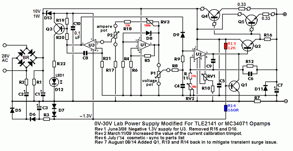
I'm planning to build (another) power supply with Q1 to see if it clamps down the output to prevent spikes when the power is shut down. I plan on using 7.5K and 240 ohm divider. With power on, the base of the transistor will be -0.03V. When the negative rail collapses, the base of Q1 will be 1.23V with approx. 5.1mA. Now I just need to pick out a good transistor for Q1.
-
I have a question about the sizing of the resistor divider for Q1 on the revised schematic. Currently it is listed as 12K and 160 Ohms. When the negative rail (-1.3V) is operating, the base voltage on Q1 will be approx. -0.7V assuming a Vdc of 39.6 on the top rail. When the power is shutting off and the negative rail collapses and goes to 0V, the transistor base will be 0.5 volts. The minimum on voltage for typical transistor( 2n2222) is 0.6V. Q1 will not have the minimum voltage to switch. Using a 12K resistor the current may not saturate the transistor to operate like a switch. The original design utilized a 5.1 zener for the negative rail with (10K and 1.5K) divider on Q1 resulted in a operating voltage on the base of the transistor of -0.01 V, but when the negative rail collapsed it resulted in 5.1V on the base of Q1. Do I have an error in my math?
-
Hi Redwire,
On the original and fixed version your diode D2 was a resistor with almost NO voltage drop. Now the D2 has a voltage drop that changes when the temperature changes then the output voltage changes when the temperature changes.
Without a negative supply for the current control opamp the output current will not be regulated when it is set to less than about 0.8V/0.27 ohms= 2.96A. The output voltage of the current control opamp must be able to go to -0.7V so that regulation at low currents works. Then its negative supply must be at least -0.9V so use two diodes like I did.
Thanks for the reply. I guess there is no getting around not having a negative charge pump with this type of design. I'm curious to see how this guy gets around the problem. Considering he is using a .1 ohm resistor, the theoretical load would be substantial before there would be stability. I think from a practical standpoint if there is a heavy load and 0.47 ohm sense reisistor, the ground for the current op amp is pushed low enough down to provide some control.
I am also going to re-look at the design on the first post here. I seemed to have the oscillation under control and I could change the voltage smoothly. I was having some current control issues in that the opamps seemed to be fighting each other until the current setting was set to its lowest setting. If I set the voltage at 14V and the current at 100mv, then connect a load of 1.5 A the current control would never kick in. It was like in a runaway mode.
-
Here is the sketch with the diode on Pin 3 to compensate for the diode drop on the current op amp. Would this work?

-
The op-amp will need a negative supply to compensate for the diode voltage drop and that of the op-amp's output stage.
Yep, your right. could you add another diode on Pin 3 of the Voltage op amp after the other diode leading to the current op amp. This way the voltage set for 0 V output is actually 0.7 on the line leading to the non inverting pin. Then the current op amp would only need to bring pin 3 the line down to 0.7?
. -
Yes I did forget to show the diode from pin 3 on the voltage Opamp to prevent positive voltage from the current op amp. The op amp (TLE2141) can handle 0-44V and sink up to 80ma. I estimate there will be no more than 8ma to sink on the current opamp and about 3ma output on the voltage op amp using the darlington transistor.
-
How about this redesign ?
-
Another question: Is the 100K resistor base resistor for Q2 (2n2222 voltage control transistor) really necessary?
-
The 100k series base resistor for the 2N2222 adds tremendous phase shift (it is feeding stray and transistor capacitance) that you do not want. The series 1k base resistor feeding the BD140 transistor also adds phase shift. But the opamp is designed so that its gain is less than 1 at a frequency where its internal phase shift causes negative feedback to become positive feedback.
The phase shifts from the two added transistors add to the opamp's internal phase shift and causes the opamp to oscillate at a lower frequency where the entire amplifier still has some gain.
Would using a voltage divider from the output of the Opamp to the 2N2222 allow a significantly lower base resistor and reduce the phase shift? Would a different transistor also help? -
Your circuit has Q1 with high voltage gain and a phase shift from R15. You also have Q2 with high voltage gain and phase shift from R13. Then you feedback the high gain and extra phase shifts to the inverting input of the opamp so it oscillates.
The original circuit used only a single driver transistor as an emitter-follower (a voltage gain of only 1) with a very small phase shift.
This is not a revision of the Power supply with 163 pages. This is a different design based on the original circuit here. Which was posted on Youtube here Although I changed some values I did not add any transistors or reconfigure the basic circuit design but I did add some caps for the op amps which gives is a design that appear to be similar to the long posted design.
Regarding high gain, if a BJT transistor is current driven wouldn't reducing the current by adding a resistor to the base also reduce the gain and negate the effects.
I found with a 10k resistor on the darlington MJ11016 and a 1.2K with the 2N5886 the oscillation ceased. I found I still needed at least a 47uf cap so I decided to keep the 100uf. So far I have gotten no other recommendation to attack the phase shift issue except redesign.
-
The new circuit oscillates because the output amplifier transistors provide too much voltage gain.
The original circuit and all the improvements until recently had only one driver transistor as an emitter follower with a voltage gain of only 1 like a piece of wire. Your new circuit has Q1 and Q2 as common emitter amplifiers feeding series resistors that add with the following capacitance which causes phase shift.
But I didn't add another driver transistor unless you are referring to the use of the MJ11016 darlington output transistor. I did try the circuit with a 2N5668 and it had the same output problems.
As long as Q1 is a common emitter amplifier there's a risk it'll oscillate, especially under certain conditions (a large capacitor connected to the output with a low ESR). This is because you've introduced another pole with a phase shift influenced by the load impedance.
http://en.wikipedia.org/wiki/Phase_margin
The original design used a 100uf cap at the output.
Initially I thought this was too high and changed this to 10uf like the other design when I had oscillations I changed it back to 100uf, but now it seems I was heading in the wrong direction and need to change it back to 10uf.
It seems having a slow output tranistor with a fast opamp can be an issue. So would using a faster power transistor help? If so, how do I choose a faster transistor from the data sheet, by the bandwidth product? a 2N3055 is listed at 6MHz, but a 2N3442G is listed at 80mHz. Would that help?
I added a 100k resistor to the base of the MJ11016 power transistor and the oscillations did stop. I will change the 100uf cap back to 10uf .
I didn't like the response on the current control and the setup with the led connected directly to the output of the opamp concerns me. It seems this indicator should be driven by a transistor. I noticed that when the inverting pin was higher than the non inverting pin the output voltage on Pin 6 would slowly decrease (over seconds) instead of nearly instant control. I may need to change C4 to 100pf instead of 220nf but I don't see that as a total fix becasue of how slow it is responding. -
Would adding a resistor to the base of Q1 (BD140) and to the base of the power transistor be a solution? What about changing to complimenary transistor set up (BD139) with a lower gain rather than the 2N2222 which has a much higher gain?
-
The other thread seems to be corrupted or locked so I will continue here
Although I had many wires and jumpers the PS seemed to work well and testing seemed good until i shorted the board and burned some traces. Happy with the design, I had 3 new boards made and populated 2 of them. Unfortunately something is not right. When there is no load, the voltage would spike up and down about once a second. If I disconnect the feedback from the power transistor to the board it will not spike. I changed C5 from 100pf to 200nf and the output was steady without a load. If set the voltage to 4V and connect a load, the output shoots up and oscillated between 35V and 17V at about 800Hz. The voltage and current regulation did not seem to work. Only if I set the current to minimum and then apply a load it will not spike and oscillate. I changed the output tranistor from the darlington to a 2N5886 and had the same results. Any suggestions.
-
Looking for suggestions. I built the board as shown in the above post with quite a few wires and jumpers and things seemed to work very well. I then had 3 boards made. I populated 2 of them. Strange things happend on the new boards. With no load the output would spike about once every second. I changed C5 to 200nf instead of 100pf and the PS worked smoothly with no load. If I set the voltage to about 4V and connect a load, the output voltage instantly surges and oscillates between max and 17v at a frequency of 800hz. Neither the voltage or current control seem to work with a load. If I set the current to minimum before attaching a load then the PS will not ramp to max and oscillate.
-
Liquibyte here are some results: The blue line is the reference voltage to the voltage control op amp and Yellow is output voltage.
NewFile 3 is startup 12v, under load
NewFile 4 is startup 12v, no load
NewFile 5 is shutdown with load (no load takes a long time to shutdown for scope)
NewFile 6 is startup 3-4v, under load


-
Your R9 82R resistor is hooked up the the wrong rail in that schematic I think. I'm also getting a lot of oscillations a low voltages when I simulate this and can't get the output to go above 12V with a load. You say you've got this built? What's the output look like on the scope at lower voltages?
If you connect the 82R resistor to the other rail then you will never measure the voltage drop across the current op amp and the PS will never current regulate.
I had 3 boards made based on the first schematic that I posted. I did notice a few problems 1) voltage drop when I added a load 2)I changed to a 10uF cap for faster response but discovered significant noise. I changed back to a 100uF and it is smooth. 3) It had some noise on pin 3 of the voltage op amp so I put a cap on it and it was quiet. 4) I initially had a cap betwen the ground and ground pin on the 10k potentimeter and that didn't work. 5) There was an grounding error on the old .brd file. As far as I know the sketch shown is correct.
I get 37V output with a 28AC transformer. If you only get 12 v then you likely have a short (or equal value) on the feed back resistors on the voltage op amp. Considering you are feeding 12V and only getting 12V out. -
After running some tests, here is the latest version. Seems to be working pretty well. I was able to set the voltage to about 3.5 V -unloaded and then put a load about 1.5A with no drop in voltage. I will continue to do more tests. I found that the leakage voltage to be about 3-4mV which is very good and the diode did nothing to change that.

-
I wanted to note that R11 (the 18K resistor) that provides negative feed back to the voltage regulator and is tied to the output side of the sense resistor. The original project shows it connected the the transformer side of the resistor. The youtube video for the original design showed a voltage drop at the output when a load was applied. I believe by moving the ground connection to the output side of the sense resistor will fix this problem.
EDIT: C5 should be 200nF
This topic is corrupted. Please continue discussion on this topic.
-
-
I used thru hole parts for this trial board. I don't see any reason why smd parts wouldn't work just fine. The only parts that get warm are the bridge diode, resistor for power on led and the .22 ohm 5W non inductive resistor when pushing a heavy load. I built the board to also fit a 10W 0.27 ohm resistor, but unless you are trying to get more than 3A the 5W resistor should be fine. Using the darlington power transistor puts very little load on the BD140. Just ordered 3 PCB's for the design shown.
-
Good News. I built the subject PS with the following changes:
1. Used 10,000uf main cap instead of 4,700 uf
2. Used TLE 2141 op amps with caps similar to Project Power supply
3. Deleted funky zener/Fet/Resistors reference voltage an used a 12V linear regulator as reference voltage for better thermal coefficient
4. Added a few other caps similar to Project Power supply.
5. Changed the value of a few resistor for a greater current range and to limit output until a trimmer can be added to negative feed back loop.
6. Used MJ11016 single output transistor.
Outcome: Using 12 v setting being controlled by current with 0.5 amp bulb I didn't see any over shoot at start up and the design has the ability to turn voltage down to less than 5mv without a load.
EDIT 11/22/14 Note that voltage dropped with load on this design. See later design
Changes still needed: the 100uF cap at the output provides sluggish voltage drop with no load. I added a 10k resistor to output which helps significantly but I intend to change the 100uF to 10uF.
Overall , very impressed with function.
NewFile12: is during shutdown
NewFile13: when plugged in with load


-
When the load current is higher than the current regulator setting and the voltage is set high, the "on" voltage spike is caused by the time it takes for the negative supply to reach a low enough voltage (-1V?) for the current regulating opamp to pull down the voltage feeding the voltage output amplifier.
Here is my proposed fix:
Yes, I agree the proposed fix would likely give rid of a lots of parts and simplify the board. When you add the two addtional transistors, is Q3 still needed or will the lower transistor connect to the led instead? One thing I am curious about is how low the output will go with the recommended arrangement when the negative rail is deleted?
While I didn't build the suggested fix, a while back I disconnected the negative rail and connected Pin 4 of U3 to ground, the minimum output voltage nearly doubled.
-
The 3A version uses two output transistors. Each emitter resistor has a max voltage of 1.5A x 0.33 ohms= 0.5V across it. When the output voltage is shorted or is low then each output transistor heats with (30V - 0.5V) x 1.5A= 44.25W.
Why do you use 30V instead of the collector voltage of approx 40V (with a 28V transformer) when computing the power? -
KINGTIGER, it appears that you don't want to use an Arduino (where only a usb cable is needed to program the chip) but rather have a ATMEGA8 in mind -perhaps because of a project you found uses one? Or, you want to do direct programming. Have you considered the 324u breakout boards from Adafruit. The 324u a broader capability than the Atmega8. You only need a USB cable (no programming board) and Studio software to program using C. It has a on board led that you can toggle to ensure your output timing is correct and you don't need to make a pcb to program it.


0-30V Stabilized Power Supply
in Projects Q/A
Posted
Dave, Can you provide a sketch showing the transistor layout between U1 and U3, as well as your modified the power supply to U1?