
spur
-
Posts
8 -
Joined
-
Last visited
Content Type
Profiles
Forums
Events
Posts posted by spur
-
-
The -1.3V supply is regulated by the two series diodes. The voltage will never go as high as -1.5V as you show.
but datasheet of 1N4148(fairchild) shows that with 30mA forward current , forward bias will be 0.8V. so the negative supply will be 1.6. I think 1.5V is reasonable. ::)
BTW, can I use my 30V 5A transformer with MC34071 or TLE2141? in your part-list the transformer is characterized 28V 4.3A !!? -
The latest version uses common and inexpensive MC34071 or TLE2141 opamps.
but my transformer is 30V 5A (although I'm not sure about 5A), can I use these opamps with this transformer?The -1.3V supply has a very low load current
the load current ( if you mean negative supply pin of U3 ) is very low, that is correct, but C3 is continuously discharging through R3 (220ohm) . with 10V across C3 the discharging current will be 39mA.
simulation results for current of R3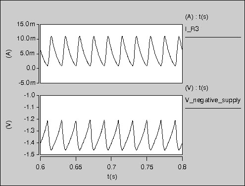
-
the output voltage might be too high the next time it is turned on
ooo! i haven't thought of that.I don't believe your simulation
I think I have to build the circuit and test the resistor values in real circuit. I'm having trouble finding OPA445, a friend of mine is going to buy them for me, but he will not come to me until two or three weeks later, so I have to wait :'(
thank you for your answers. I really enjoy reading your posts in this forum. -
Hi
what happens if I remove R1? what if I increase the value of R2 to say 560 ohm? (in that case I can use a 1/4 watt or 1/2 watt resistor.)
I simulated the circuit, the lower waveform is -1.3V line, the upper waveform is the voltage across C2. the black waveform is for R2=82ohm and the red waveform is for R2=400ohm.
you can see that increasing R2 affects charging voltage of C2 (I think that's because time constant of RC circuit rises and in a short time, C2 cannot charge to its MAX voltage, am I correct?).
can anyone explain to me why discharging voltage level of C2 is independent of R2 ? discharging current of C2 is also goes through R2, so why is that the final value of the voltage across C2 is the same with both small and large value of R2?
thanks. -
R16 shunts the collector-base leakage current away from the base.
The datasheet for a 2N3055 transistor shows that its maximum collector to emitter leakage current is 0.7mA when it has a Vce of 30V, it is at 25 degrees C and it has no base current with its base not connected.
thanks audioguru :)
OK! here is my problem
0.7mA * 1Kohm = 0.7V , R16 shunts the base-emitter junction of Q4, so there is 0.7V across base-emitter, so the transistor turns on. ???
am i wrong?
i did a few searches over the internet and found out that Icer (a resistor between base and emitter - just like this) is more useful in understanding the real performance of a transistor, but i don't understand why we tend to define something like Icer (instead of Iceo) and why it is more useful??
and I couldn't find any good article or webpage to describe the concept of Icer.
-
Hi,
what is the role of R16 ? ;D ;D
I know that it has been asked by some people before, and here is the answers:R16 turns off the output transistor, and does it quickly.
Without it, the project's output voltage would probably rise if it is powering a low-current load, because of the leakage current in Q2 and Q4. The leakage current is fairly high because the transistors operate hot in this project.
R16 speeds-up the turn off because it discharges the capacitance of Q4 quickly.R16 bypasses any leakage current in Q4 when it gets hot to turn it off when it is supposed to conduct a small current.
OK! but i can't get it clearly ::) ??? :-\
how does it bypass the leakage current?
does the leakage current passing through Q4 causes the Q4 to turn off?
does flowing the leakage current into C7 rises the output voltage?
can anyone clearly show (or characterize) this leakage current?
... and questions like that ;) ::)
I'll appreciate it if anyone take the time to answer my questions.
and ... it is obvious that my English is not good :-[ . apologies.
Need some interesting usage of electronics in agriculture
in Electronics chit chat
Posted
Hi,
Does anyone knows some of the amazing applications of electronics in agriculture?
I'll be grateful if anyone could help me find some. Of course I need some technical (or detailed) information about those applications.
thanks guys.