

sofiatian
-
Posts
4 -
Joined
-
Last visited
Content Type
Profiles
Forums
Events
Everything posted by sofiatian
-
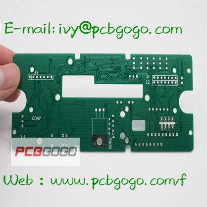
hello everyone, Here i'd like to recommend a pcb manufacturer to you----PCBGOGO PCBGOGO Circuits is one of the most experienced PCB manufacturers in China. We're manufacture high-quality PCBs and PCB assembly. Now register on our website, you will get $100 coupon . www.pcbgogo.com/f You also can send me your file via email for inquiry: [email protected] In PCBGOGO you can enjoy best service. * 12/24 hours express for PCB prototype * 24hours customer service available Live on-site * 99% + on-time DHL delivery * Guaranteed quality from quote to delivery * Professional PCB engineer one-to-one service. * Instant quote online & order procedure tracking * Delivery shorted from 2-4days by DHL
-
How do you go about designing your own PCB? The ins and outs of PCB design are way too in depth to get into here, but if you really want to get started, here are some pointers: 1. Find a CAD package: there are a lot of low-cost or free options out there on the market for PCB design. Things to consider when choosing a package: 2. Community support: are there a lot of people using the package? The more people using it, the more likely you are to find ready-made libraries with the parts you need. 3. Ease-of-use: if it’s painful to use it, you won’t. 4. Capability: some programs place limitations on your design- number of layers, number of components, size of board, etc. Most of them allow you to pay for a license to upgrade their capability. 5. Portability: some free programs do not allow you to export or convert your designs, locking you in to one supplier only. Maybe that’s a fair price to pay for convenience and price, maybe not. 6. Look at other people’s layouts to see what they have done. Open Source Hardware makes this easier than ever. 7. Practice, practice, practice. 8. Maintain low expectations. Your first board design will have lots of problems. Your 20th board design will have fewer, but will still have some. You’ll never get rid of them all. 9. Schematics are important. Trying to design a board without a good schematic in place first is an exercise in futility. 10. Finally, a few words on the utility of designing your own circuit boards. If you plan on making more than one or two of a given project, the payback on designing a board is pretty good- point-to-point wiring circuits on a protoboard is a hassle, and they tend to be less robust than purpose-designed boards. It also allows you to sell your design if it turns out to be popular. hope that will be helpful. PS: is there anyone ever used pcbgogo? the pcb manufacturer offer pcb prototype service.really recommend .if you have pcbs need to facbricate,maybe you can try ,www.pcbgogo.com/f
-
Q: At a fixed board size, if the design need to accommodate more functionality, they often need to increase the density of PCB traces, but this can lead to mutual interference traces enhanced while the traces are too small to make impedance can not be reduced, may I ask what skill at high speed (> 100MHz) high density PCB design? A: in the high-speed high-density PCB design, the crosstalk (crosstalkinterference) really should pay special attention because of its timing (timing) and signal integrity sex (signalintegrity) has a great influence. Here are a few caveats: 1. Continuous control go and match the characteristic impedance of the line. 2. trace spacing size. General often see a pitch twice the width. Can Through simulation to know trace spacing on timing and signal integrity, and to find the minimum distance can be tolerated. Results of different signals may be different chips. 3. Select the appropriate termination method. 4. Avoid vertically adjacent layers of the same alignment direction, even just walking up and down the line overlap together, because this case crosstalk traces larger than the layer adjacent to the same. 5. The use of blind and buried vias (blind / buriedvia) to increase the alignment area. However, pcb board production costs will increase. In the actual implementation does not perfectly parallel to the same length, but still want to try to do. In addition, you can reserve a differential and common mode termination termination, to ease the impact on the timing and signal integrity. i worked in pcbgogo , is a chinese Custom PCB Prototype Manufacturer, and our factory's Site Engineer told me more about pcbs design .so there i'd like to share with you . www.pcbgogo.com/f On the selection and wiring hybrid circuit PCB material : Q: In today's wireless communication device, a radio frequency part often using small outdoor unit structures, while the RF part of the outdoor unit, the IF section, and the outdoor unit to monitor low-frequency circuit section often deployed on the same PCB. Will such a PCB layout on the material requirements? How to prevent interference with radio frequency, intermediate frequency and low frequency circuits between each other? A: hybrid circuit design is a big problem, it is difficult to have a perfect solution. Usually RF circuits in the system are carried out as an independent board layout, and even have a special shield cavity. And RF circuits are generally single-sided or double-sided, the circuit is simple, all of which is to reduce the impact on the distribution parameters of the RF circuit, improve the consistency of RF systems. With respect to the general FR4 material, RF board and the substrate tends to use high Q value of the dielectric constant of this material is relatively small, distributed capacitance smaller transmission line impedance is high, small-signal transmission delay. In the hybrid circuit design, although the RF, digital circuitry to do in the same piece PCB, but are generally divided into the RF circuit area and the digital circuit region, respectively layout. Between grounding and shielding box via tape shield.
-
PCBGOGO -Custom PCB Prototype Manufacturer ,is provide the best ever service in quick-turn PCB prototype, low & medium volume and low cost.The best PCB(printed circuit board) buying experience in the country today .PCBGOGO is committed to provide short and accurate lead time for PCB manufacturing job.The quickest lead time PCBGOGO can do is 12hours. And PCBGOGO has Instant online quote and detailed tracking system which will inform you the each process of the PCB boards. www.pcbgogo.com/f And now big promotion is coming.don't miss it.