Search the Community
Showing results for tags 'driver'.
-
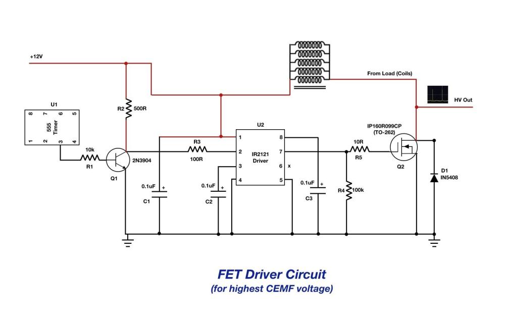
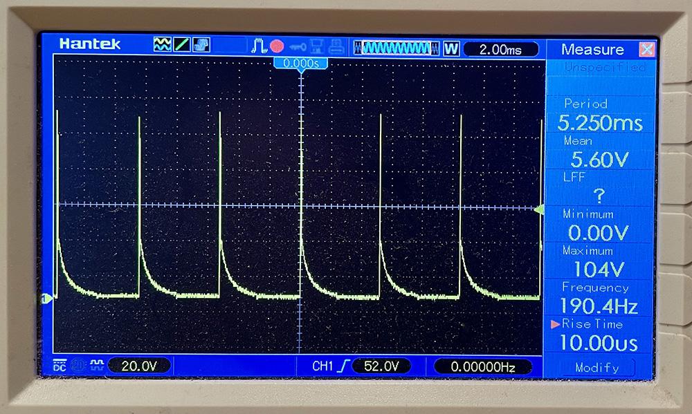
I have built a circuit for which the aim is to produce high voltage back EMF spikes from the Drain of a MOSFET so I can investigate some of the properties of these voltage transients. What I have built is shown in the attached circuit where I am using an IR2121 driver chip to encourage shorter shut off times and so produce higher voltage spikes. Going from a circuit that didn't use a driver chip to one that does has increased the voltage from about 800V to 1,040V as shown in the scope image using a 10:1 voltage divider. I have read that there are ways to further reduce the FET shut off time but as electronics is not my main discipline I find them rather confusing. For example, reducing the Gate bias resistor (R5) further (to 5R?) or putting a small capacitor (1nF?) across R5 and keeping the PCB track resistance from R5 to the Gate of Q2 as short as possible. I would appreciate any suggestions. Thanks
-
Hi, all I'm using a PCA9685 with a pinout board like Adafruit's. I'm trying to run a bunch of LEDs at 20 mA, and the chip is supposed to be able to source 10 mA and sink 25 mA. I understand that to have it Source, you connect the LED between the PWM and GND pins and to Sink you connect it between V+ and PWM. I've tried both ways and using a multimeter and a red LED I get 12.5 mA. Why is it not 25 in Sink? Also, why do I get 12.5 on Source mode as well? Is there anyone have ideas of it? if possible a simple explanation would be nice. Many thanks.☺️
-
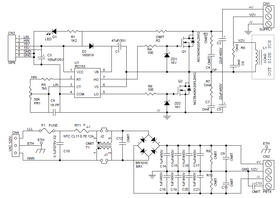
Hi. I am going to try this circuit in the link. But With this circuit what I didn't understand is ground symbols. Where are they connected exactly(not the ETH I know it is for earthing). For the second circuit +V and -V connections are clear but 1/2V is connected to ground through the middle of rectifier capacitors. Should I connect it to somewhere or is it just for reference. And for the first circuit CN1 and CN2 are connected together respectively and -V is connected to ground symbol. And again is it a reference for us to connect it with ground of 15V dc? I am new to this forum. I searched and I didn't see any topic regarding this. Thank you for reading.
-
Has someone the new datasheet from the JYQD_V7.3E3 motordriver (24V) (that one with the hall sensor pads on the side and not the regular one that it is aligned) DC-12-V-36-V-15A-500W-Senza-Spazzola-Del-Motore-Sala-BLDC-Bordo-di-Driver.jpg_640x640q70.jpg_.webp
- 6 replies
-
- motor driver
- driver
- (and 4 more)


