Search the Community
Showing results for tags 'pcb design'.
Found 6 results
-
 With the rapid development of the Internet of Things, more and more intelligent products such as intelligent home, intelligent transportation, intelligent city and so on have emerged in the market. These terminals rely on wireless transceiver module to realize information transmission and reception. As a result, we know that wireless modules are indispensable in the use of the Internet of Things.Wireless modules often need a backplane to match them, enabling them to perform better in their application.So the design of our backplane is particularly important. How to design is our concern. Today, let's briefly talk about how to design the backplane of our wireless module. Most importantly, we should pay attention to the space reserved for wireless modular antennas. Our most common antennas are ceramic antennas, PCB loaded antennas, and external antennas (just a generic name here). External Antenna Fig.1 is a typical external antenna-based wireless module backplane design.From Fig.1, Fig.2, we can see that on the left are USB interface, LDO, plug-in interface, Jing Zhen, USB-TTTL chip, module bottom without components and line. When we design the module, we try not to walk high-speed lines and place components sensitive to RF signals. The module is placed in a separate area to prevent interference with other functional modules from causing communication problems. The outboard antenna SMA is on the far right, preventing the effects of RF signals on other sensitive devices after they are radiated through the antenna. As we can see from Fig.3, when we draw the RF line from the base plate to the outside SMA head, the RF line needs to have an accompanying hole, which allows a vortex between the RF signal and the ground, a circuit in space, to absorb part of the radiated signal, thereby reducing the effect of radio-frequency signal radiation on other signals inside the plate.Another reason is the Faraday shield, together with a hole that effectively prevents other signals from interfering with it. Ceramic Antenna, PCB Board Antenna Ceramic antennas and PCB loaded antennas are similar in design. This is the unified explanation here. From Fig.4, we can see that the left side is the same design as Fig.1. This is no longer the case here, but focus on the placement of the right antenna. We can see that when we are designing, we need to place ceramic antennas at the edge of the board (sometimes because of some restrictions, the antenna needs to be placed inside the backplane, then we need to carve out the position of the antenna and hang the antenna outside the backplane so that the antenna can radiate out the radio signal better and communicate better. Of course, there are more factors involved in baseplate design, which requires a combination of actual conditions and often a compromise.
 -
 Choosing the right Surface Finish for Chip on Board assembly is crucial. One of the most frequent questions we are asked at KingCredie Technologies is how should my PCB be plated in order to ensure wire bond-ability. PCB Plating for Chip on Board Assembly must be planned in advance to ensure manufacturability of the device. This planning begins with design rules and selecting the wire bond method to be used. Common wire bond materials include aluminum or gold wire. Aluminum Wedge Wire Bonding and ENIG Plating One of the most common wire bond methods for COB assembly is aluminum wire bonding. For aluminum wire bonding to a PCB the plating can be a low cost method known as ENIG or Electroless Nickel with Immersion Gold. With ENIG plating a PCB with Copper traces is plated with a Nickel layer and then the nickel layer has a flash gold layer on top. The Flash Gold is a barrier layer to protect the Nickel from oxidation. The wire bonding connection is actually from the aluminum wire to the Nickel plating. The main advantage of this method is inexpensive plating and relatively easy wire bonding. The disadvantage is Aluminum wire bonding is less flexible than gold bonding and generally requires larger bond pad pitch compared to gold bonding. Gold Ball Wire Bonding and soft gold plating For Gold Ball Bonding to Printed Circuit Boards a thick layer of soft gold has traditionally been required. In this Case the copper traces on the PCB are plated with a nickel layer and then a soft gold layer measuring between 15 and 30 micro-inches. The gold is electroplated and when plated correctly provides an excellent surface for wire bonding. This method has the advantage allowing for fine pitch gold ball bonding. The disadvantages are high cost and the thick gold layer can cause reliability problems with surface mounted components due to gold dissolution into the solder. Gold Ball Wire Bonding with ENEPEG plating In recent years Electroless Nickel, Electroless Palladium, Immersion Gold plating has been proven to be the best compromise between cost and manufacturability. This method of plating is known and ENEPIG and is common referred to as the universal plating method. It is called universal plating because it offers good wire bond ability and good solder ability. It is suitable for RoHS solders as well as Eutectic SnPb solder. The typical plating thickness is 100 to 150 micro inches of nickel followed by 4 – 10 micro inches of palladium followed by 1-2 micro inches of gold. ENEPIG is suitable for both Gold and Aluminum wire bonding. Additionally, With recent increases in the price of gold price to levels above US$1200 per troy oz, the production cost of electronic device that required thick gold electroplating becomes extremely difficult to control. Since the cost of palladium metal has remained relatively low in comparison to gold, an opportunity for cost saving by replacement of gold with palladium is now available. At KingCredie for PCB plating with Chip on Board we recommend using ENEPIG as a preferred plating method.For more information,tell us what you want to know.
-
 This is a question always been asked so I try to make this list to cover as many pcb manufacturers as I can. This is a listing of websites making PCBs and also may including PCBAs. I will try to update the infomation now and then. http://www.pcbway.com/ -$5!!! http://www.pcbgeek.com/ http://www.sfcircuits.com http://expresspcb.com/ http://www.apcircuits.com/ http://www.10pcb.com/ http://www.goldphoenixpcb.com/ http://batchpcb.com/index.php/Products http://www.pad2pad.com/index.html http://www.pcbcart.com./ http://www.4pcb.com/ http://www.pcbfinpo.com/ http://www.sunstone.com/ http://www.pmsnewzealand.com/ http://www.ezpcb.com/ezpcbweb3/index.php http://dorkbotpdx.org/wiki/pcb_order http://pcbconnect.com/index.html http://www.screamingcircuits.com/Order/ http://www.pcborder.com/site_new/default.asp http://www.custompcb.com/ http://www.multi-circuit-boards.eu/?gclid=CK20v5fFga4CFYZN3godg1in6Q http://iteadstudio.com/store/index.php?cPath=19_20 https://www.itead.cc/open-pcb/pcb-prototyping.html http://www.seeedstudio.com/depot/fusion-pcb-service-p-835.html?cPath=185 http://imall.iteadstudio.com/open-pcb/pcb-prototyping.html?p=2&price=-100 - $0.2 !!! https://ecommerce.pcbfabexpress.com/ http://www.goldphoenixpcb.com/ http://oshpark.com https://www.protoexpress.com/ - SierraCircuits http://www.4pcbassembly.com/ http://www.mitchelectronics.co.uk/ http://www.customcircuitboards.com/ http://dirtypcbs.com/ http://www.elecrow.com/special-offer-for-2-layer-1010cm-max-green-pcb-510pcs-p-761.html http://pcbshopper.com/ http://smart-prototyping.com/PCB-Prototyping.html http://www.technotronix.us/ http://www.pcbunlimited.com/ http://store3.sure-electronics.com/ The list is not in any priority. I've never ordered board from any houses. I've just made board with the first two entries. This is a "work in progress". New board houses may be added, along with some comments.
- 13 replies
-
- 1
-

-
- pcb list
- pcb manufacturing
- (and 2 more)
-
 Hi all, I found a ver very good and really cheap pcb service! Its called PCBWay, and they have cheap 2layer 10x 10x10cm pcb for just $5! and shipping to the Netherlands was just $7!(china post) And they have real good and very kind customer service witch reply back very fast and every question i had got answered in not time AND they give you $5 free for your first order! Pcb's look good and came fast. All pcb's where exported with eagle. I got 2 extra pcb's(win win) probably if a pcb fails check or something. I used blue silkscreen with white text for the pcb and also bought some project pcb's with holes wich i got in 5 collors and look absolutly great! The blue silkscreen looks absolutly perfect, its really perfectly alligned! and the text looked good, it looked a little bit blocky but still it looks great! I ordered pcb's for a adafruit solar charger clone as i needed 9 of them and just didnt have the money to buy them. Since i already had all the components i needed exept the pcb's i just bought the pcb's since their charger is opensource and created them my self to save some costs.(i'll probable sell the last one i dont need) At first i thought if i had to buy the comonents also it all would be more expensive but i calculated if i wanted to create 10 solar chargers and bought all components from aliexpress and bought the pcbs from pcbway i save around $30 to my suprise!!!!!(first time self build a product is cheaper then buying) The chargers are for my solar powered raspberry pi zero powered wireless timelapse and livestream camera's, witch will be mounted in my backyard pointing at bird homes and one as security camera for my back yard gate to watch intruders. I already finished one of the charger and it looks really really impressive with the blue silkscreen! I'll maybe upload some pics of my assembled pcb's and bare pcb's soon for other peaple to check and i am probably going to clone the adafruit powerboost 1000 charger too!(because its cheaper offcourse, i still bought a lot of products from adafruit so i am still supporting them). The pcb's are of good quality, no broken or half traces, all boards are straight and not bend, all boards got the silkscreen and white text right so they just look amazing! I really really recommend this service to everyone and i am defenitly going to try their 4 layer too some time!! And they also offer cheap assembly services so maybe i will try that sometime too! Since i am very very and very happy with my pcb's i am defenitly buying from them again and again in the future and recommend them to everyone! So now i want to know who else used this service and had good experience or wants to try it out? hope to hear from you all!
 -
 How do you go about designing your own PCB? The ins and outs of PCB design are way too in depth to get into here, but if you really want to get started, here are some pointers: 1. Find a CAD package: there are a lot of low-cost or free options out there on the market for PCB design. Things to consider when choosing a package: 2. Community support: are there a lot of people using the package? The more people using it, the more likely you are to find ready-made libraries with the parts you need. 3. Ease-of-use: if it’s painful to use it, you won’t. 4. Capability: some programs place limitations on your design- number of layers, number of components, size of board, etc. Most of them allow you to pay for a license to upgrade their capability. 5. Portability: some free programs do not allow you to export or convert your designs, locking you in to one supplier only. Maybe that’s a fair price to pay for convenience and price, maybe not. 6. Look at other people’s layouts to see what they have done. Open Source Hardware makes this easier than ever. 7. Practice, practice, practice. 8. Maintain low expectations. Your first board design will have lots of problems. Your 20th board design will have fewer, but will still have some. You’ll never get rid of them all. 9. Schematics are important. Trying to design a board without a good schematic in place first is an exercise in futility. 10. Finally, a few words on the utility of designing your own circuit boards. If you plan on making more than one or two of a given project, the payback on designing a board is pretty good- point-to-point wiring circuits on a protoboard is a hassle, and they tend to be less robust than purpose-designed boards. It also allows you to sell your design if it turns out to be popular. hope that will be helpful. PS: is there anyone ever used pcbgogo? the pcb manufacturer offer pcb prototype service.really recommend .if you have pcbs need to facbricate,maybe you can try ,www.pcbgogo.com/f
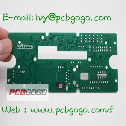
-
Q: At a fixed board size, if the design need to accommodate more functionality, they often need to increase the density of PCB traces, but this can lead to mutual interference traces enhanced while the traces are too small to make impedance can not be reduced, may I ask what skill at high speed (> 100MHz) high density PCB design? A: in the high-speed high-density PCB design, the crosstalk (crosstalkinterference) really should pay special attention because of its timing (timing) and signal integrity sex (signalintegrity) has a great influence. Here are a few caveats: 1. Continuous control go and match the characteristic impedance of the line. 2. trace spacing size. General often see a pitch twice the width. Can Through simulation to know trace spacing on timing and signal integrity, and to find the minimum distance can be tolerated. Results of different signals may be different chips. 3. Select the appropriate termination method. 4. Avoid vertically adjacent layers of the same alignment direction, even just walking up and down the line overlap together, because this case crosstalk traces larger than the layer adjacent to the same. 5. The use of blind and buried vias (blind / buriedvia) to increase the alignment area. However, pcb board production costs will increase. In the actual implementation does not perfectly parallel to the same length, but still want to try to do. In addition, you can reserve a differential and common mode termination termination, to ease the impact on the timing and signal integrity. i worked in pcbgogo , is a chinese Custom PCB Prototype Manufacturer, and our factory's Site Engineer told me more about pcbs design .so there i'd like to share with you . www.pcbgogo.com/f On the selection and wiring hybrid circuit PCB material : Q: In today's wireless communication device, a radio frequency part often using small outdoor unit structures, while the RF part of the outdoor unit, the IF section, and the outdoor unit to monitor low-frequency circuit section often deployed on the same PCB. Will such a PCB layout on the material requirements? How to prevent interference with radio frequency, intermediate frequency and low frequency circuits between each other? A: hybrid circuit design is a big problem, it is difficult to have a perfect solution. Usually RF circuits in the system are carried out as an independent board layout, and even have a special shield cavity. And RF circuits are generally single-sided or double-sided, the circuit is simple, all of which is to reduce the impact on the distribution parameters of the RF circuit, improve the consistency of RF systems. With respect to the general FR4 material, RF board and the substrate tends to use high Q value of the dielectric constant of this material is relatively small, distributed capacitance smaller transmission line impedance is high, small-signal transmission delay. In the hybrid circuit design, although the RF, digital circuitry to do in the same piece PCB, but are generally divided into the RF circuit area and the digital circuit region, respectively layout. Between grounding and shielding box via tape shield.