12V DC @ 120mA – 1.4W Universal Input Buck Converter – 85V AC – 265V AC INPUT
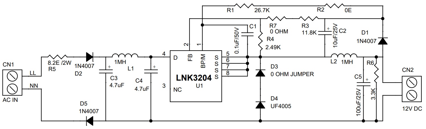
The circuit shown in the schematic below is a typical implementation of a 12 V – 120 mA non-isolated power supply that can be used in appliance control such as rice cookers, dishwashers, or other white goods. This circuit may also be applicable to other applications such as night-lights, LED drivers, electricity meters, and residential heating controllers, where a non-isolated supply is acceptable.
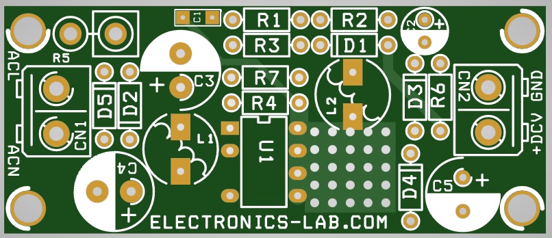
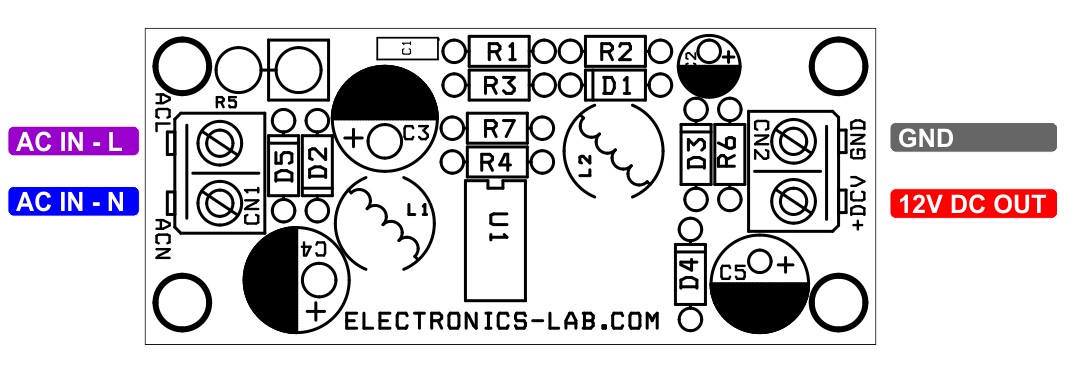
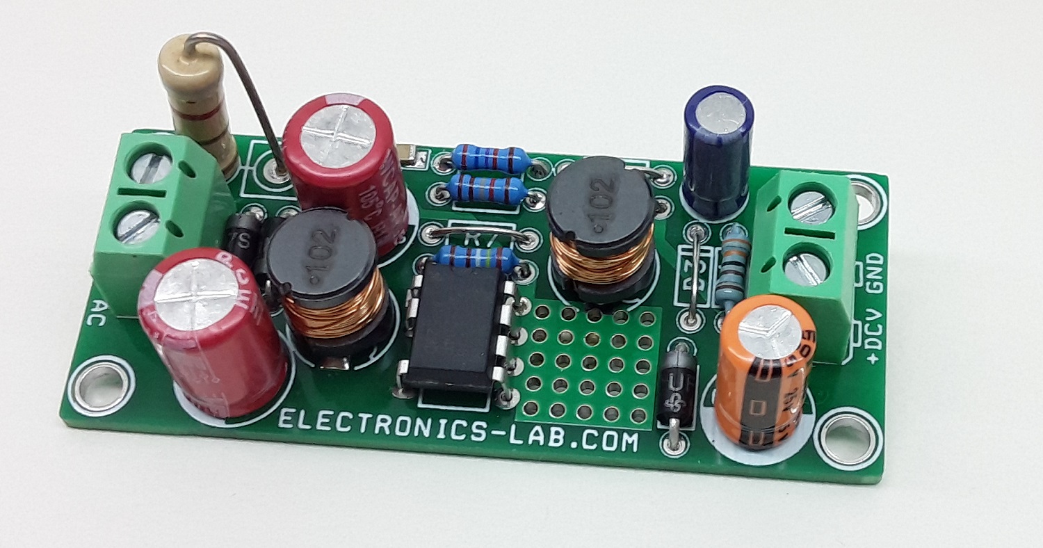
Resistor R5 controls inrush current at a safe level for D2/D5, D2/D5 converts AC supply into DC, inductor L1 for EMI noise, Capacitor C3-C4 DC filter capacitor. The power processing stage is formed by the Link-Switch, freewheeling diode D4, output choke L2, and the output capacitor C5. The LNK3204 was selected such that the power supply operates in the mostly discontinuous mode (MDCM). Diode D4 is an ultrafast diode with a reverse recovery time of approximately 75 ns, acceptable for MDCM operation. For continuous conduction mode (CCM) designs. Inductor L2 is a standard off-the-shelf inductor with an appropriate RMS current rating (and acceptable temperature rise). Capacitor C5 is the output filter capacitor; its primary function is to limit the output voltage ripple. The output voltage ripple is a stronger function of the ESR of the output capacitor than the value of the capacitor itself. Optional resistor R1 supplies the BYPASS pin externally for significantly lower no-load input power and increased efficiency over all load conditions.
To first order, the forward voltage drops of D1 and D4 are identical. Therefore, the voltage across C4 tracks the output voltage. The voltage developed across C4 is sensed and regulated via the resistor divider R3 and R4 connected to U1’s FEEDBACK pin. The values of R3 and R4 are selected such that, at the desired output voltage, the voltage at the FEEDBACK pin is 2.00 V. Regulation is maintained by skipping switching cycles. As the output voltage rises, the current into the FEEDBACK pin will rise. If this exceeds IFB then subsequent cycles will be skipped until the current reduces below IFB. Thus, as the output load is reduced, more cycles will be skipped, and if the load increases, fewer cycles are skipped. To provide overload protection if no cycles are skipped during a 50 ms period, Link-Switch IC will enter auto-restart, limiting the average output power to approximately 3% of the maximum overload power. Due to tracking errors between the output voltage and the voltage across C2 at light load or no-load, R6 provided for a small pre-load.
Features
- Input Supply 85V AC To 265V AC
- Output 12V DC @ 120mA
- Screw Terminals for AC Input and DC Output Connections
- Frequency 66Khz Operates with Accurate Current Limit
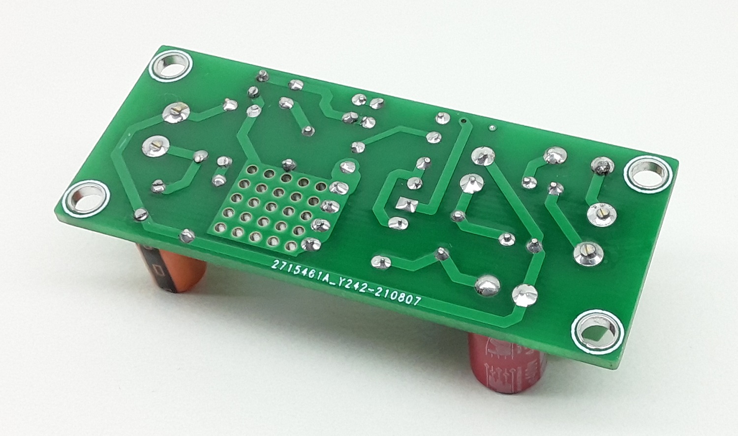
- PCB dimensions: 60.96 x 25.72 mm
Schematic
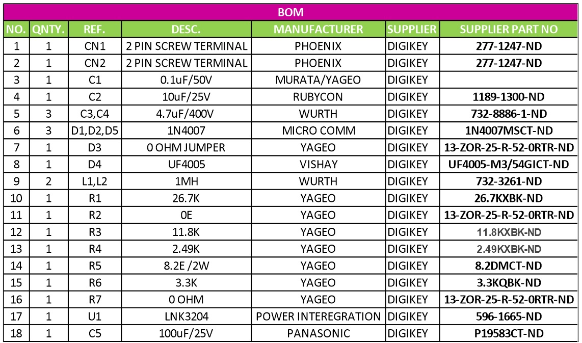
Parts List
| NO. | QNTY. | REF. | DESC. | MANUFACTURER | SUPPLIER | SUPPLIER PART NO |
|---|---|---|---|---|---|---|
| 1 | 1 | CN1 | 2 PIN SCREW TERMINAL | PHOENIX | DIGIKEY | 277-1247-ND |
| 2 | 1 | CN2 | 2 PIN SCREW TERMINAL | PHOENIX | DIGIKEY | 277-1247-ND |
| 3 | 1 | C1 | 0.1uF/50V | MURATA/YAGEO | DIGIKEY | |
| 4 | 1 | C2 | 10uF/25V | RUBYCON | DIGIKEY | 1189-1300-ND |
| 5 | 3 | C3,C4 | 4.7uF/400V | WURTH | DIGIKEY | 732-8886-1-ND |
| 6 | 3 | D1,D2,D5 | 1N4007 | MICRO COMM | DIGIKEY | 1N4007MSCT-ND |
| 7 | 1 | D3 | 0 OHM JUMPER | YAGEO | DIGIKEY | 13-ZOR-25-R-52-0RTR-ND |
| 8 | 1 | D4 | UF4005 | VISHAY | DIGIKEY | UF4005-M3/54GICT-ND |
| 9 | 2 | L1,L2 | 1MH | WURTH | DIGIKEY | 732-3261-ND |
| 10 | 1 | R1 | 26.7K | YAGEO | DIGIKEY | 26.7KXBK-ND |
| 11 | 1 | R2 | 0E | YAGEO | DIGIKEY | 13-ZOR-25-R-52-0RTR-ND |
| 12 | 1 | R3 | 11.8K | YAGEO | DIGIKEY | 11.8KXBK-ND |
| 13 | 1 | R4 | 2.49K | YAGEO | DIGIKEY | 2.49KXBK-ND |
| 14 | 1 | R5 | 8.2E /2W | YAGEO | DIGIKEY | 8.2DMCT-ND |
| 15 | 1 | R6 | 3.3K | YAGEO | DIGIKEY | 3.3KQBK-ND |
| 16 | 1 | R7 | 0 OHM | YAGEO | DIGIKEY | 13-ZOR-25-R-52-0RTR-ND |
| 17 | 1 | U1 | LNK3204 | POWER INTEREGRATION | DIGIKEY | 596-1665-ND |
| 18 | 1 | C5 | 100uF/25V | PANASONIC | DIGIKEY | P19583CT-ND |
Connections
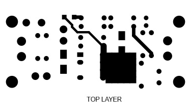
Gerber View
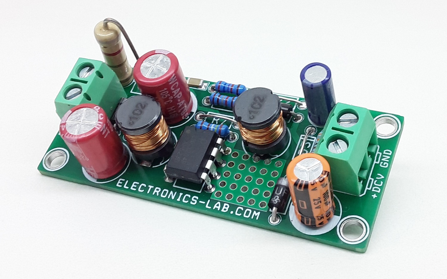
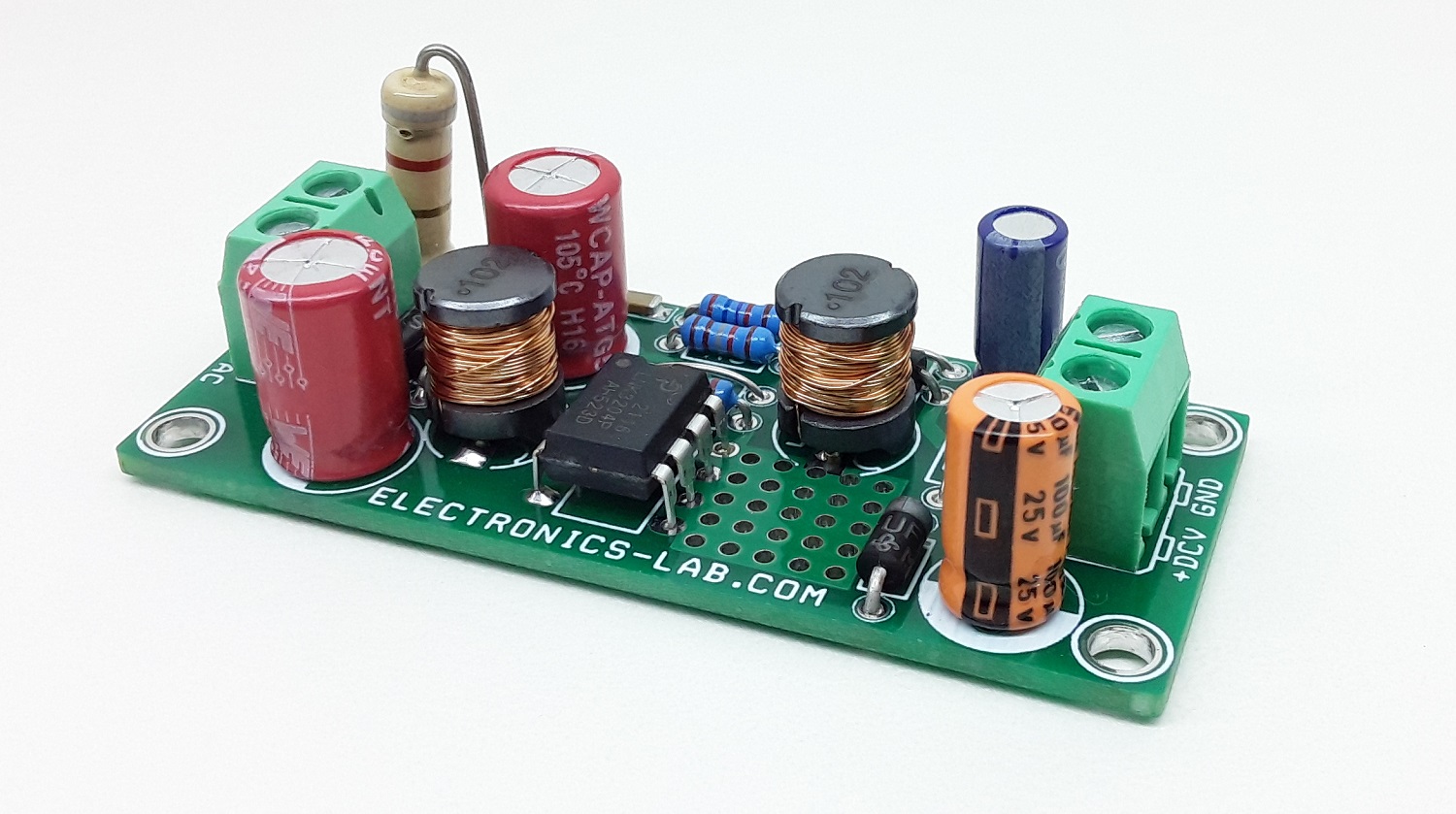
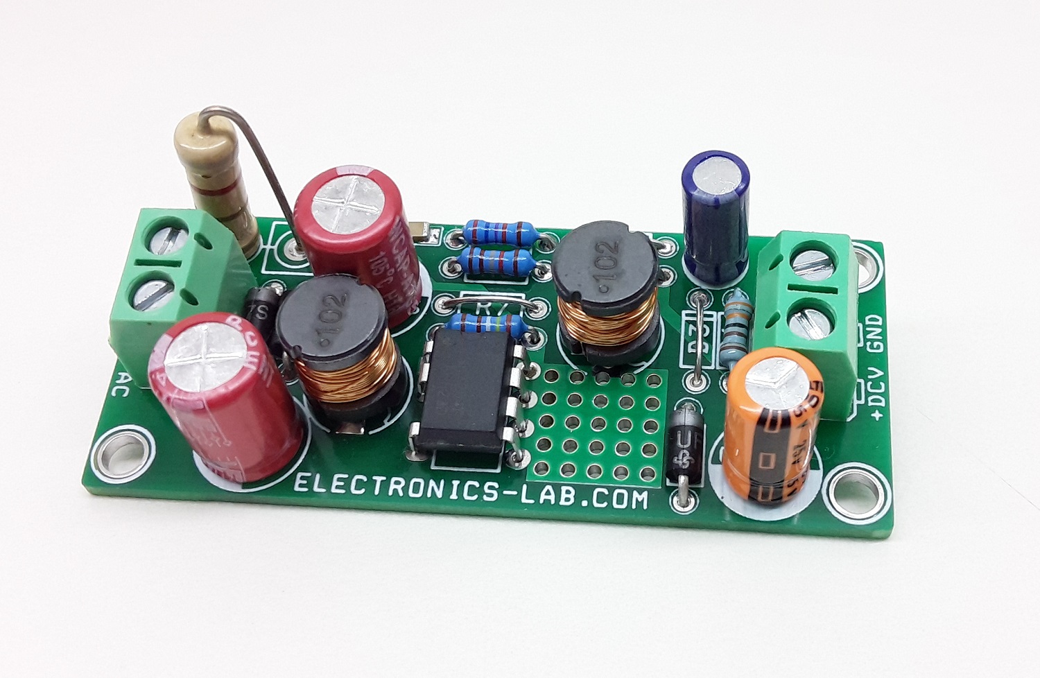
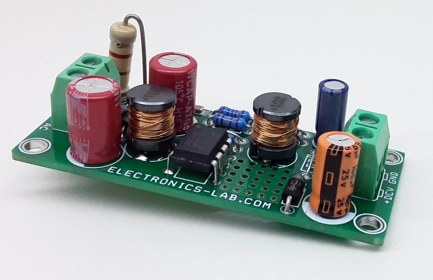
Photos
Video
LNK3204P Datasheet
PCB