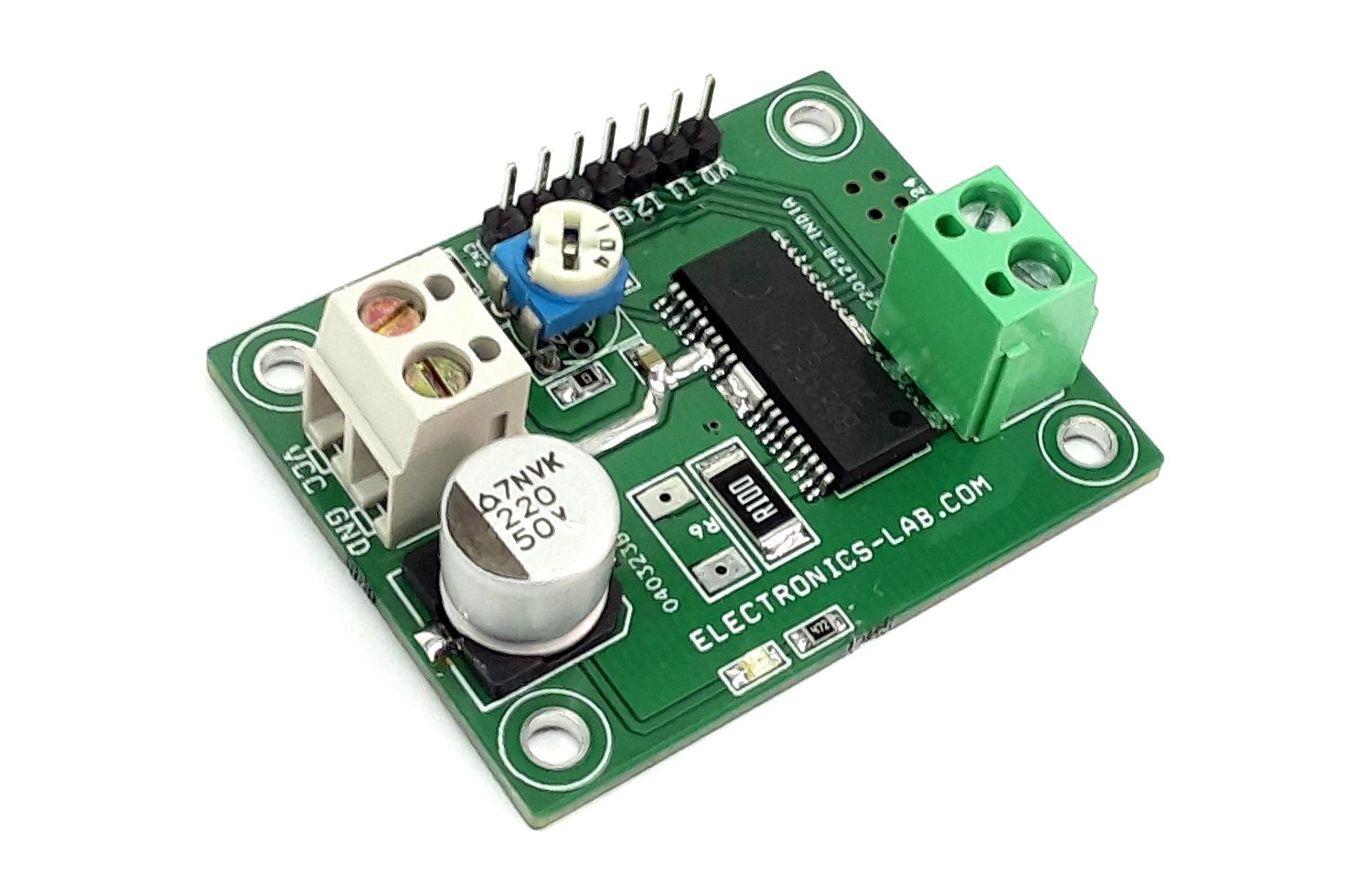
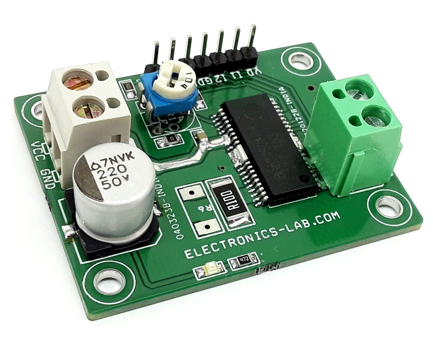
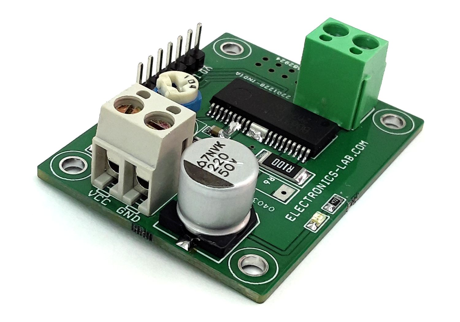
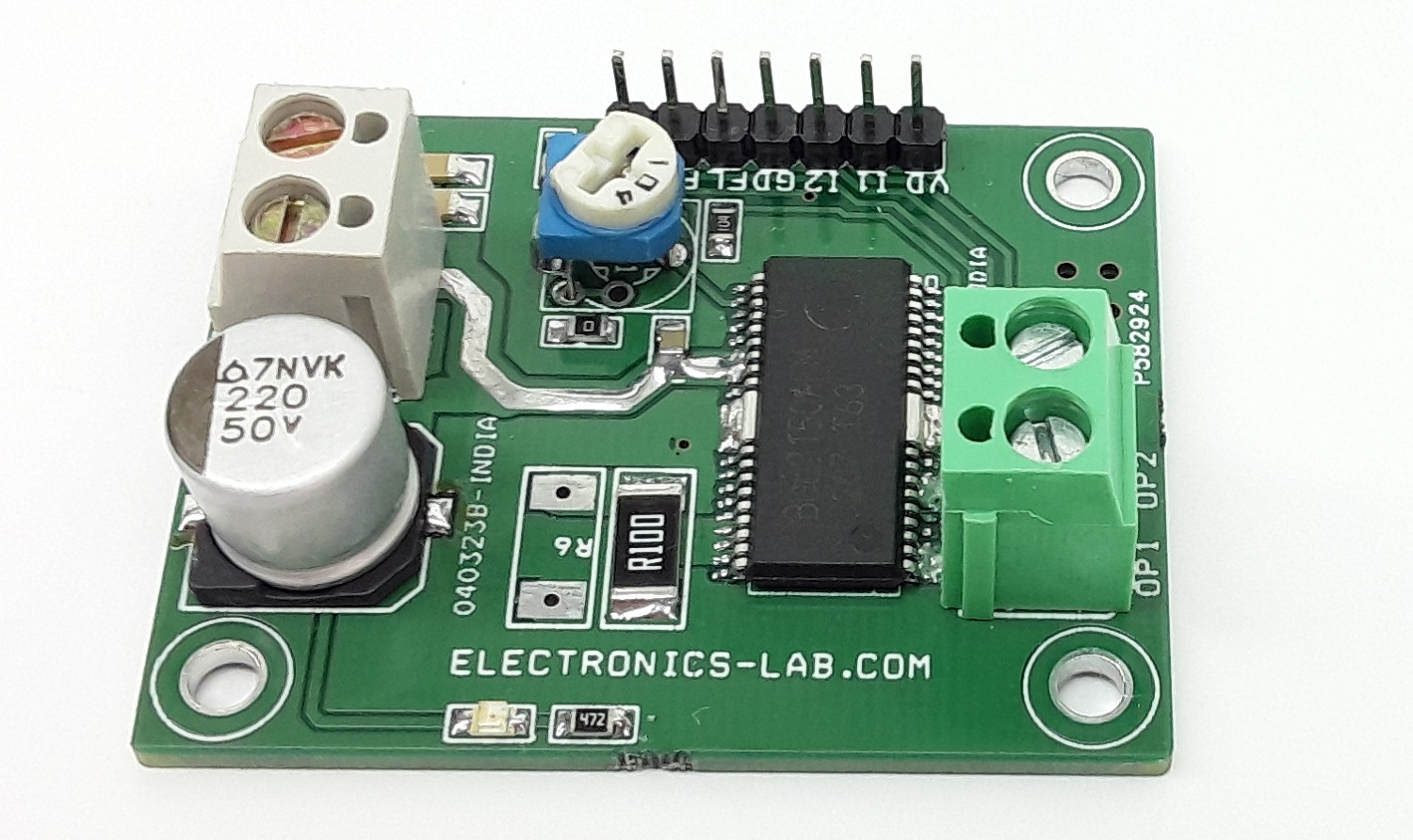
50V – 5A DC Brush Motor Driver – High Performance, High Reliability
- Rajkumar Sharma
- 152 Views
- moderate
- Tested
- SKU: EL135068
- Quote Now
- 0 Likes

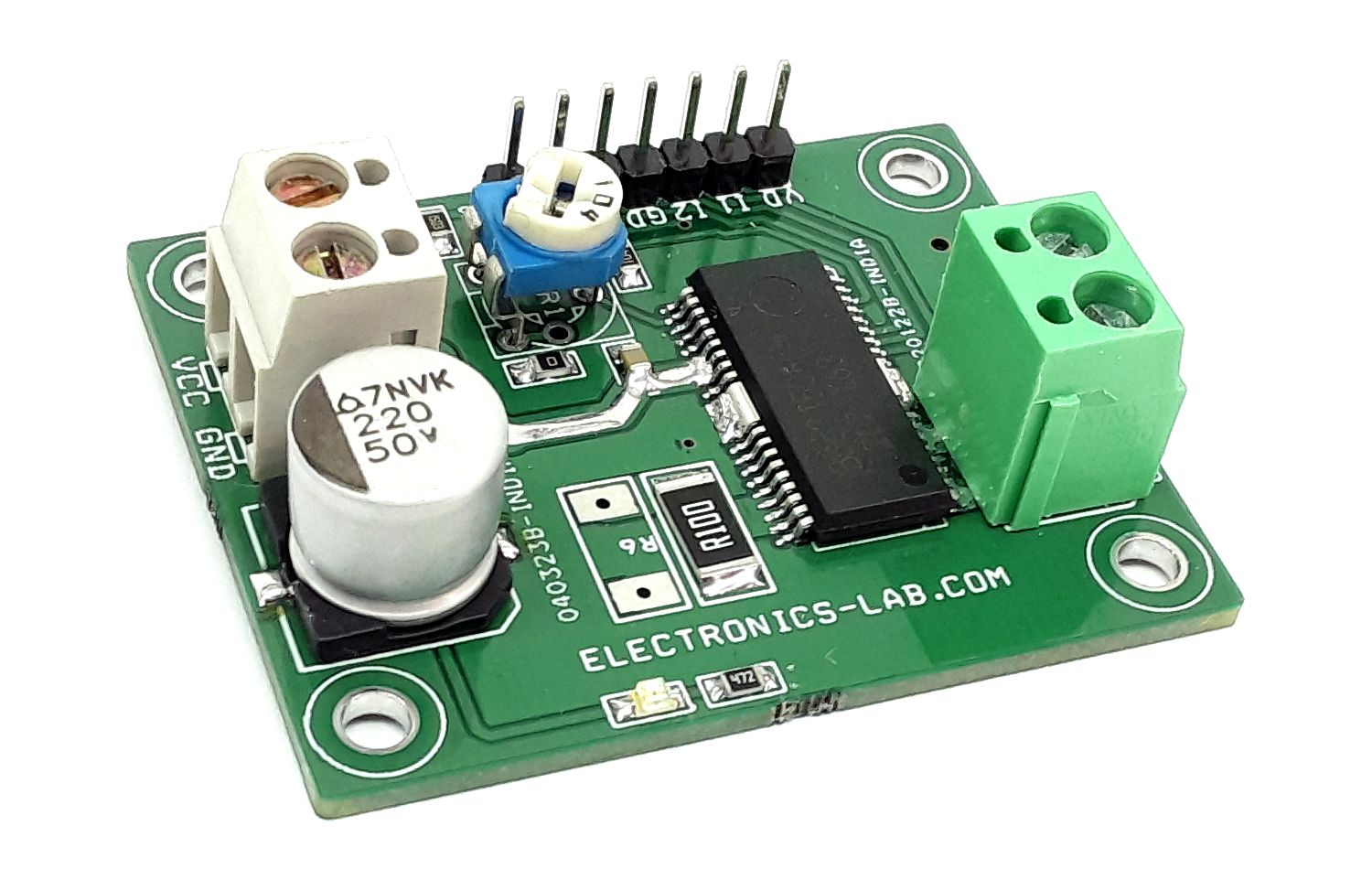
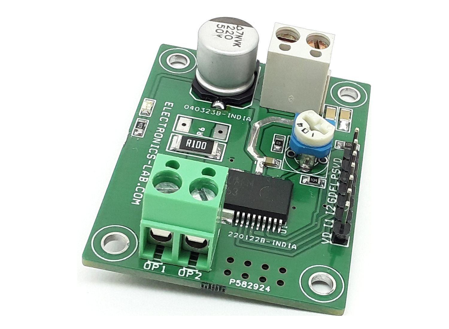
This is a powerful yet small-size and low-profile brushed DC motor drive system, with key features like adjustable constant current control, direction control, brake controls, Alert output, PWM for speed control, etc. The BD63150AFM chip is the heart of the project which is one H-bridge motor driver for DC brush motors. This board enables low power consumption by direct PWM or PWM constant current control. Built-in protection circuits in this IC are present. It is possible to output an abnormal detection signal for Wired-OR that notifies each protection circuit operation, and this contributes to the high reliability of this board.
Constant Current Mode or Direct PWM Mode Selection
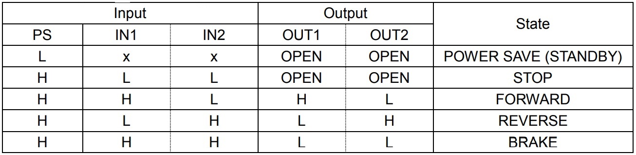
- Constant Current Mode: By default, this project works in constant current mode. Constant current can be set using Trimmer Potentiometer PR1. Use Input1 and Input2 of CN2 to control Motor Forward, Reverse, and Brake. Please refer to Table 1 for input logic.
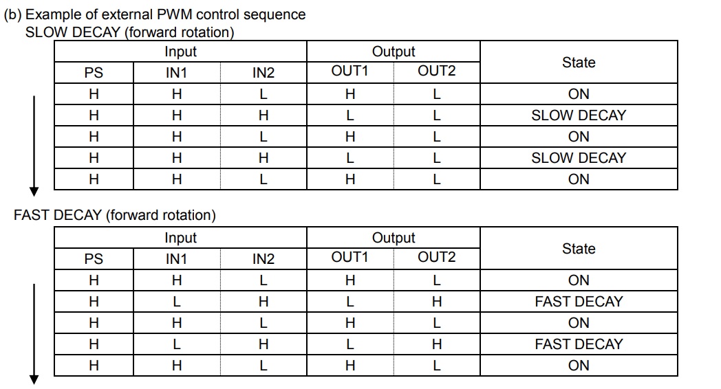
- PWM Mode: Replace resistor R1 with 0 Ohms. Adjust the PR1 trimmer potentiometer to 1 to 2V. Use Input1 and Input 2 as external PWM/Logic Input with Maximum Allowable PWM frequency 100Khz. Refer to Table 4 for the input signals diagram.
Features
- Single Power Supply Input Range 8 to 46V DC (rated voltage of 50V)
- Rated Output Current (peak): 5.0A(6.0A)
- Low ON-Resistance DMOS Output
- Forward, Reverse, Brake, Open Function
- Power Save Function
- External PWM Control – PWM Control Mode
- PWM Constant Current Control Adjustable (current limit function)
- Built-in Spike Noise Cancel Function (external noise filter is unnecessary)
- Built-in Logic Input Pull-down Resistor
- Cross-conduction Prevention Circuit
- Output Detection Signal during Abnormal states (Wired-OR)
- Thermal Shutdown Circuit (TSD)
- Over-current Protection Circuit (OCP)
- Under Voltage Lock out Circuit (UVLO)
- Over Voltage Lock out Circuit (OVLO)
- Ghost Supply Prevention (protects against malfunction when power supply is disconnected)
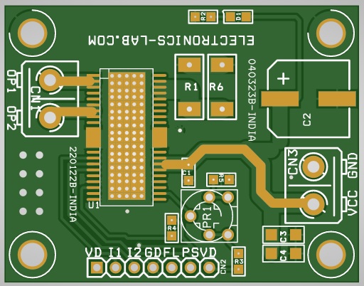
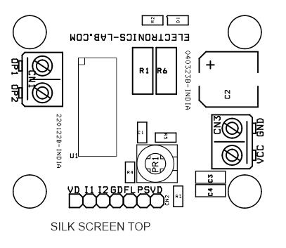
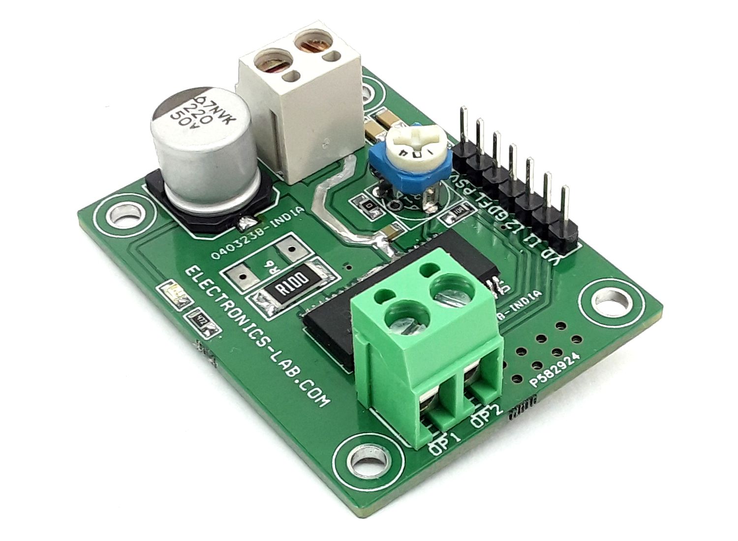
- PCB Dimensions 48.10 x 37.62mm
- Four Mounting Holes 3mm each
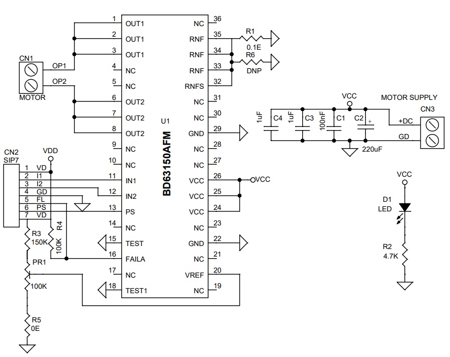
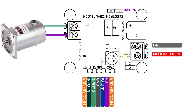
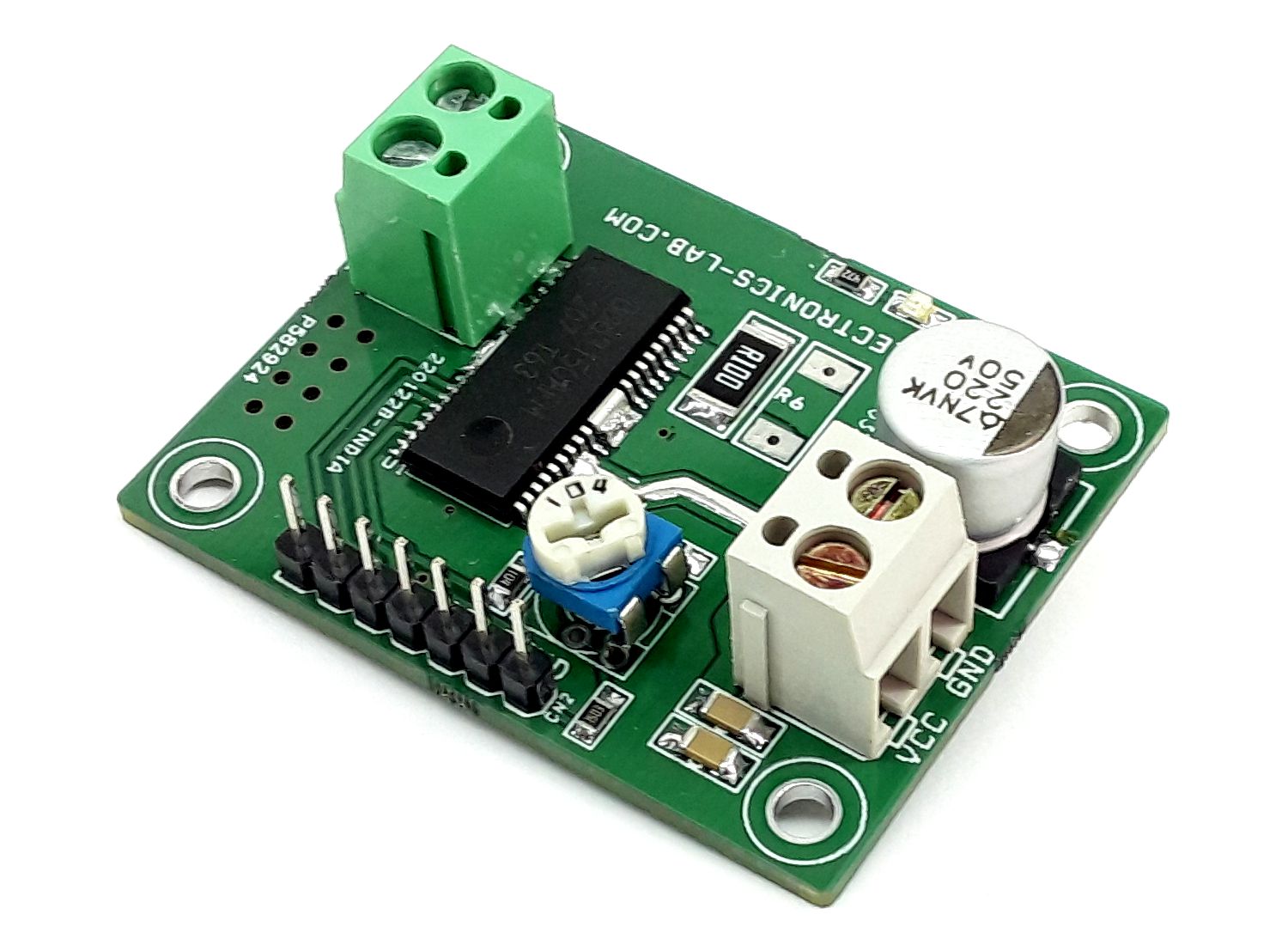
Inputs and Outputs CN2
- Pin1: VDD 5V DC @ 10-20mA- Input
- Pin2: Input 1 PWM Input or Logic High/Low input Constant Current Mode
- Pin3: Input 1 PWM Input or Logic High/Low input Constant Current Mode
- Pin4: GND
- Pin5: Fault
- Pin5: PS
- Pin7: VDD 5V DC @ 10-20mA- Input
CN3 Motor Supply Input
- Pin1: +DC 8 to 46V Motor Supply
- Pin2: GND
CN4 DC Bushed Motor
- Pin1: Motor 1 (Output1)
- Pin2: Motor 2 (Output2)
Trimmer Potentiometer PR1
- Constant Current Adjust
LED D1: Power LED
PS/ Power Save Pin Low=Power Same Mode Standby Mode, High=Active
PS can put the circuit into a standby state and make motor outputs OPEN. Be careful because there is a delay of 40μs(Max), as PS=L→H, until it is returned from standby state to normal state and the motor output becomes ACTIVE.
Input1 and Input2 (Refer Table-1)
IN1, IN2/ H-Bridge Control Pin It decides the output logic for the H-bridge
FAILA/ Fault Signal Output Pin (Refer Table -2)
FAILA outputs an abnormality detection signal when Over-Current Protection (OCP) or Thermal Shutdown (TSD) operates. Even if Under Voltage Lock Out (UVLO) or Over Voltage Lock Out (OVLO) operates, the FAILA signal doesn’t turn an abnormality detection signal (i.e., high). This signal can be connected to the microcomputer and the system can be shut down. This pin is an open drain type, and a Pull-up resistor R4 is used. Normal output is High, this pin goes low when a fault condition arises.
Thermal Shutdown (TSD)
This IC has a built-in Thermal Shutdown circuit for thermal protection. When the IC’s chip temperature rises 175°C (Typ) or more, the motor output becomes OPEN. Also, when the temperature returns to 150°C (Typ) or less, it automatically returns to normal operation. However, even when TSD is in operation, if heat is continued to be applied externally, heat overdrive can lead to destruction.
Over-Current Protection (OCP)
This IC has a built-in Over-Current Protection circuit as a provision against destruction when the motor outputs are shorted to each other or VCC-motor output or motor output-GND is shorted. This circuit latches the motor output to OPEN condition when the regulated current flows for 4μs (Typ). It returns with power reactivation or a reset of the PS pin. The over-current protection circuit aims to prevent the destruction of the IC only from abnormal situations such as when motor output is shorted and it is not meant to be used as protection or security for the device. Therefore, the device should not be designed to make use of the function of this circuit. After OCP operation, if abnormal situations continue and are returned by power reactivation or reset of the PS pin happens repeatedly, then OCP operates constantly. The IC may generate heat or otherwise deteriorate. When the L value of the wiring is great due to the wiring being long, if the output pin voltage jumps up and the absolute maximum values may be exceeded after the overcurrent has flowed, there is a possibility of destruction. Also when the current which is the output current rating or more and the OCP detection current or less flows, the IC can heat up to Tjmax=150°C or more and can deteriorate, so the current which exceeds the output rating should not be applied.
Under Voltage Lock Out (UVLO)
This IC has a built-in Under Voltage Lock Out function to prevent false operations such as IC output during power supply under voltage. When the applied voltage to the VCC pin goes 5V (Typ) or less, the motor output is set to OPEN. This switching voltage has a 1V (Typ) hysteresis to prevent false operation by noise etc. Be aware that this protection circuit does not operate during power save mode.
Over Voltage Lock Out (OVLO)
This IC has a built-in Over Voltage Lock Out function to protect the IC output and the motor during power supply overvoltage. When the applied voltage to the VCC pin goes 52V (Typ) or more, the motor output is set to OPEN. This switching voltage has a 1V (Typ) hysteresis and a 4μs (Typ) mask time to prevent false operation by noise etc. Although this over-voltage-locked-out circuit is built-in, there is a possibility of destruction if the absolute maximum value for power supply voltage is exceeded. Therefore, the absolute maximum value should not be exceeded. Be aware that this protection circuit does not operate during power save mode.
Ghost Supply Prevention (protects against malfunction when the power supply is disconnected)
If a control signal (IN1, IN2, PS, and VREF) is applied when there is no power supplied to the IC, there is a function that prevents a malfunction where voltage is supplied to the power supply of this IC or other IC in the set via the electrostatic destruction prevention diode from these input pins to the VCC. Therefore, there is no malfunction in the circuit even when voltage is supplied to these input pins while there is no power supply.
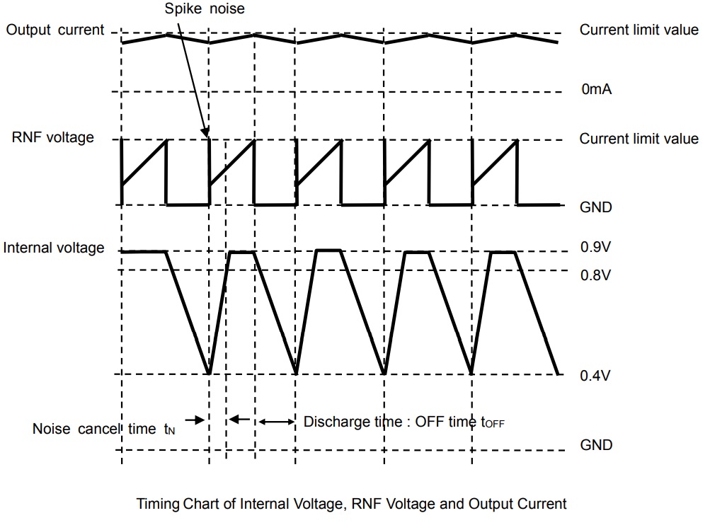
PWM Constant Current Control (refer to Table 3)
This function can limit the peak current such as switching current in driving the DC brush motor.
- Current Control Operation The output current increases due to the output transistor being turned on. When the voltage on the RNF pin, the output current is converted due to connecting the external resistance to the RNF pin, reaches the voltage value set by the VREF input voltage, and the current limit comparator engages and enters the current decay mode. Thereafter the output turned on again after a period of time determined the CR pin. The process repeats itself constantly.
- Blank Time (Fixed in Internal Circuit) In order to avoid misdetection of the current detection comparator due to RNF spikes that occur when the output turns ON, the internal voltage between 0.4V and 0.8V is provided as minimum ON time (tONMIN 1.5µs Typ). During this time, the current detection is disabled after the output transistor is turned on. This allows for the constant-current drive without the need for an external filter.
- Internal Timer (Fixed in Internal Circuit) Repeat charging and discharging between 0.4V to 0.9V internal voltage determined by IC internal circuit. When internal voltage is changed charge from discharge, the output is then ON from the current decay mode.
Schematic
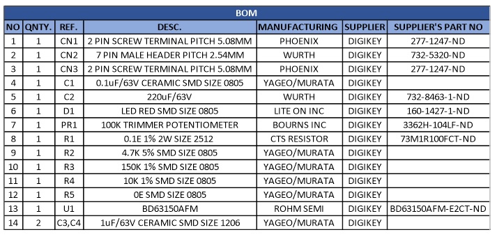
Parts List
| NO | QNTY. | REF. | DESC. | MANUFACTURING | SUPPLIER | SUPPLIER'S PART NO |
|---|---|---|---|---|---|---|
| 1 | 1 | CN1 | 2 PIN SCREW TERMINAL PITCH 5.08MM | PHOENIX | DIGIKEY | 277-1247-ND |
| 2 | 1 | CN2 | 7 PIN MALE HEADER PITCH 2.54MM | WURTH | DIGIKEY | 732-5320-ND |
| 3 | 1 | CN3 | 2 PIN SCREW TERMINAL PITCH 5.08MM | PHOENIX | DIGIKEY | 277-1247-ND |
| 4 | 1 | C1 | 0.1uF/63V CERAMIC SMD SIZE 0805 | YAGEO/MURATA | DIGIKEY | |
| 5 | 1 | C2 | 220uF/63V | WURTH | DIGIKEY | 732-8463-1-ND |
| 6 | 1 | D1 | LED RED SMD SIZE 0805 | LITE ON INC | DIGIKEY | 160-1427-1-ND |
| 7 | 1 | PR1 | 100K TRIMMER POTENTIOMETER | BOURNS INC | DIGIKEY | 3362H-104LF-ND |
| 8 | 1 | R1 | 0.1E 1% 2W SIZE 2512 | CTS RESISTOR | DIGIKEY | 73M1R100FCT-ND |
| 9 | 1 | R2 | 4.7K 5% SMD SIZE 0805 | YAGEO/MURATA | DIGIKEY | |
| 10 | 1 | R3 | 150K 1% SMD SIZE 0805 | YAGEO/MURATA | DIGIKEY | |
| 11 | 1 | R4 | 10K 1% SMD SIZE 0805 | YAGEO/MURATA | DIGIKEY | |
| 12 | 1 | R5 | 0E SMD SIZE 0805 | YAGEO/MURATA | DIGIKEY | |
| 13 | 1 | U1 | BD63150AFM | ROHM SEMI | DIGIKEY | BD63150AFM-E2CT-ND |
| 14 | 2 | C3,C4 | 1uF/63V CERAMIC SMD SIZE 1206 | YAGEO/MURATA | DIGIKEY |
Connections
Timing Diagram
Input/Output Logic

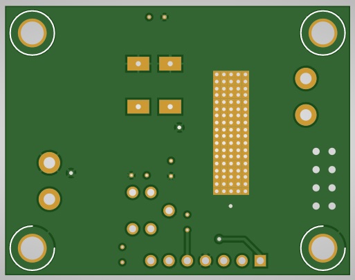
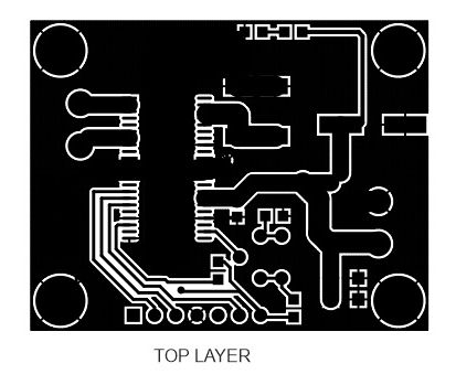
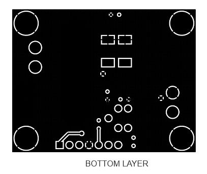
Gerber View
Photos
Video
BD63150AFM Datasheet
PCB