

Balanced Line Driver for High Speed Digital and Video Signal
The project presented here is a differential driver for the transmission of high-speed signals over low-cost twisted pair or coaxial cables. The project was built using the AD8132 chip. It can be used to transmit either analog or digital video signals or another high-speed data transmission. The board is capable of driving either a Category 3 or Category 5 twisted pair or coaxial cable with minimal line attenuation. It is capable of operating with a 10 meters of Category 5 cable.
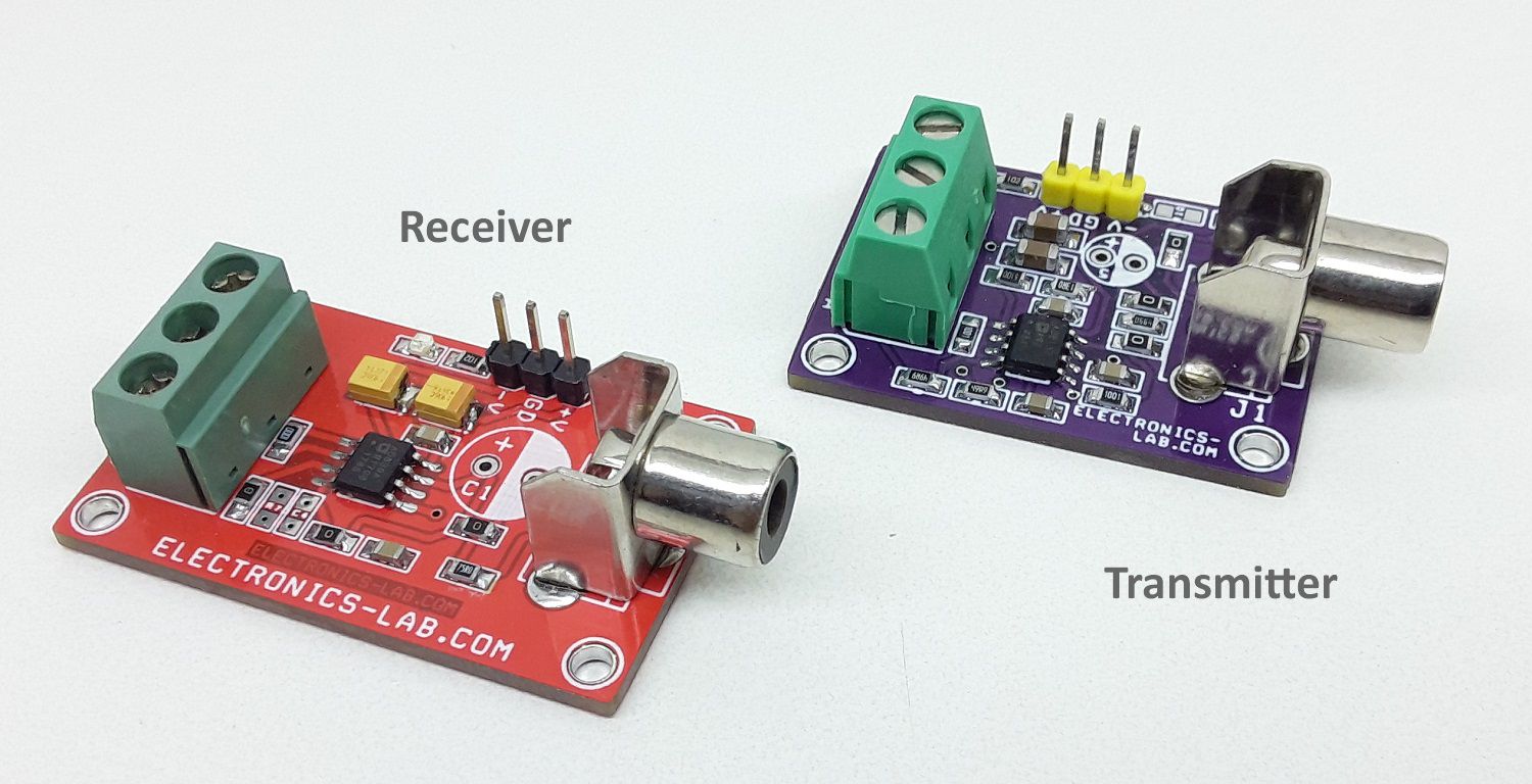
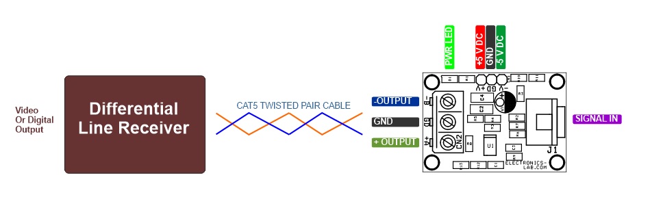
This board converts single-ended Video/Digital signals into a balanced output that can be paired with “Balanced Line Receiver for Digital Signal Over Twisted Pair CAT-5 Cable” as the receiver, published on our website.
This board has adjustable gain. You may also refer to a similar project “Single-ended Video/Digital input to differential output driver (High Speed Differential Driver)” with fixed gain published on our website.
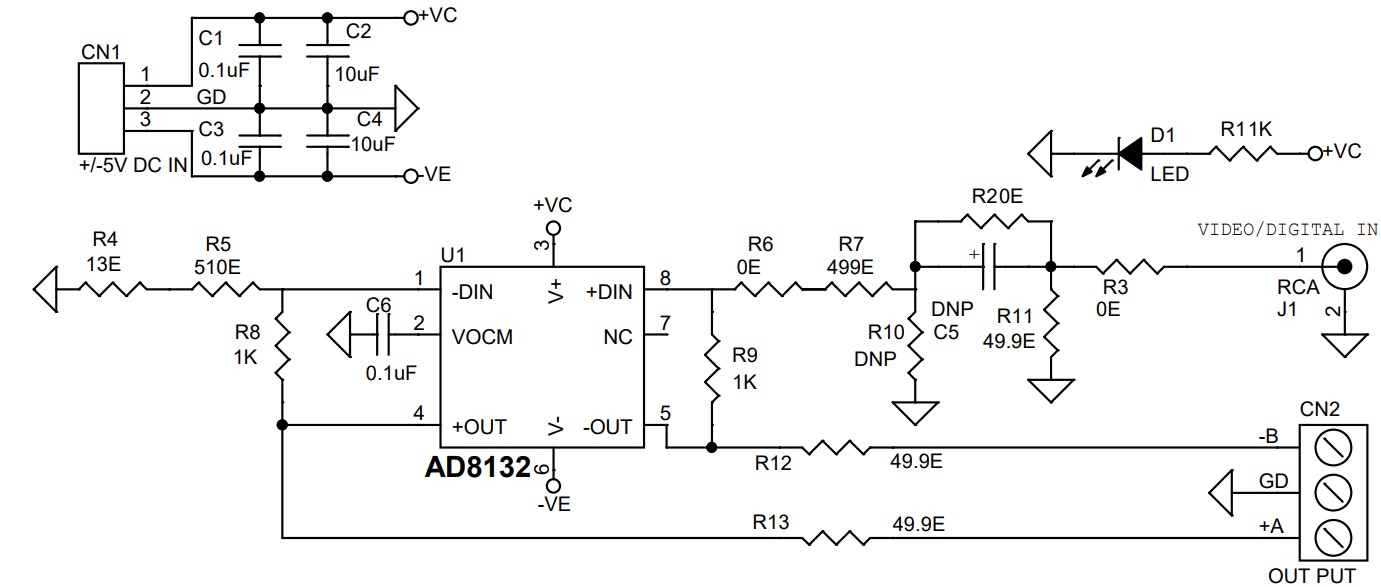
Gain Setting: Default gain is G= +2, refer to the datasheet of AD8132 to learn more about gain settings and gain change. Resistors R4, R5, R8, and R9 are used for gain adjustment.
Features
- Power supply +/-5V DC (Range: +2.7 V to ±5.5 V)
- Low power: 20 mA @ 5 V
- Maximum Output Swing +/-3.6V
- High speed 350 MHz, −3 dB bandwidth
- 1200 V/μs slew rate
- Resistor set gain (Resistor R8 and R9) Default Gain G=+2
- Internal common-mode feedback
- Improved gain and phase balance: −68 dB @ 10 MHz
- Separate input to set the common-mode output voltage
- Low distortion: −99 dBc SFDR @ 5 MHz, 800 Ω load
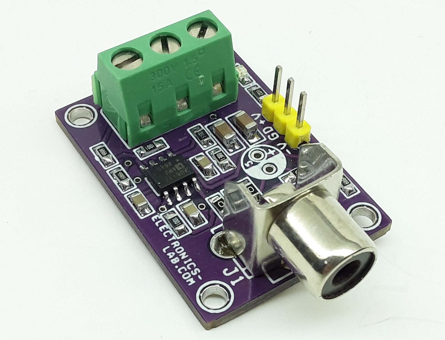
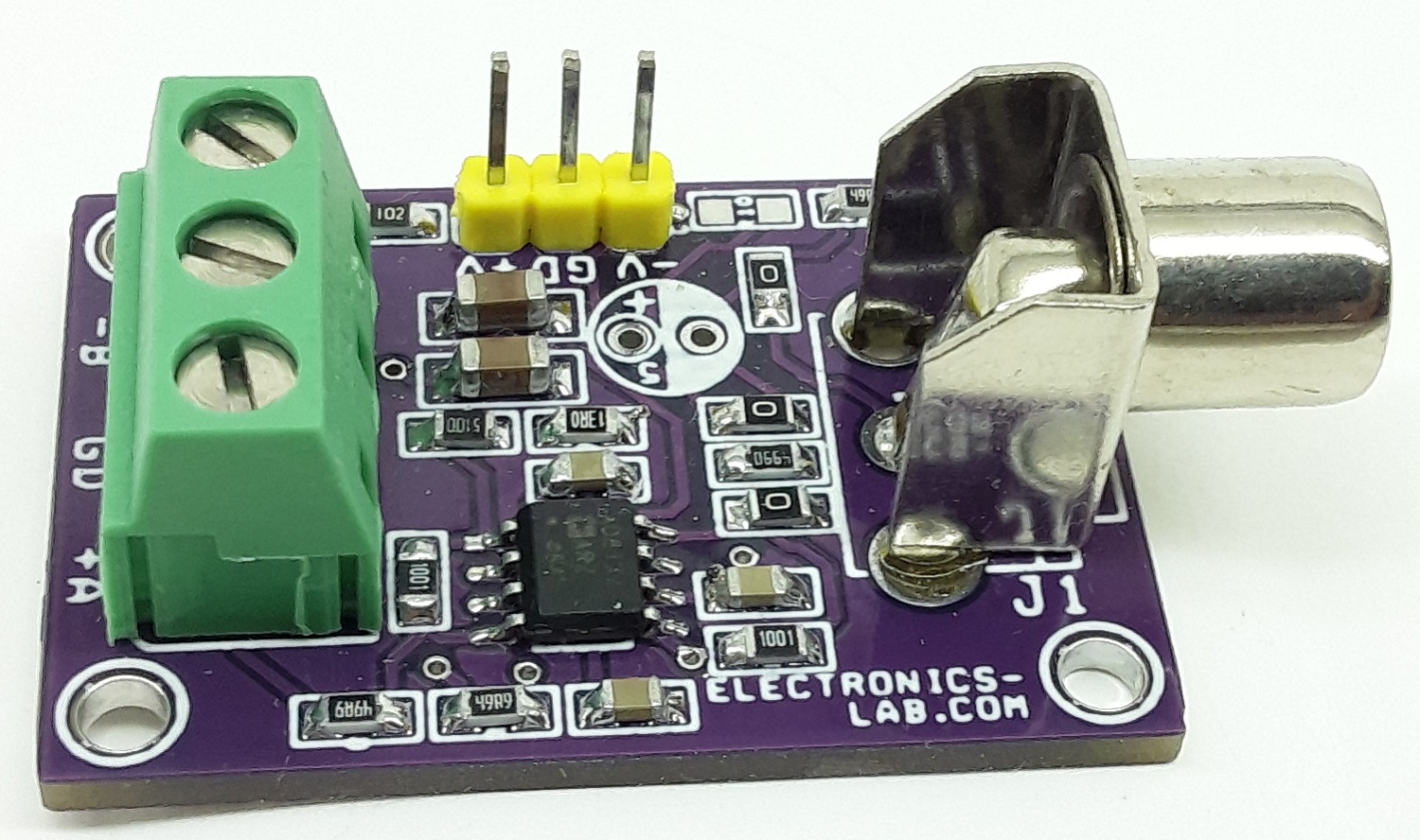
- PCB Dimensions 36.04 x 25.08 mm
The AD8132 is a low-cost differential or single-ended input to differential output amplifier with resistor set gain. The AD8132 is a major advancement over op amps for driving differential input ADCs or for driving signals over long lines. The AD8132 has a unique internal feedback feature that provides output gain and phase matching balanced to −68 dB at 10 MHz, suppressing harmonics and reducing radiated EMI.
Manufactured using the next-generation of Analog Devices, Inc., XFCB bipolar process, the AD8132 has a −3 dB bandwidth of 350 MHz and delivers a differential signal with −99 dBc SFDR at 5 MHz, despite its low cost. The AD8132 eliminates the need for a transformer with high-performance ADCs, preserving the low frequency and dc information. The common-mode level of the differential output is adjustable by applying a voltage on the VOCM pin, easily level-shifting the input signals for driving single-supply ADCs. Fast overload recovery preserves sampling accuracy.
Differential signal processing reduces the effects of ground noise that plagues ground-referenced systems. The AD8132 can be used for differential signal processing (gain and filtering) throughout a signal chain, easily simplifying the conversion between differential and single-ended components.
Advantages of Balanced Cable Driver
When driving a twisted pair cable, it is desirable to drive only a pure differential signal onto the line. If the signal is purely differential (that is, fully balanced), and the transmission line is twisted and balanced, there is minimum radiation of any signal. The complementary electrical fields are confined mostly to the space between the two twisted conductors and do not significantly radiate out from the cable. The current in the cable creates magnetic fields that radiate to some degree. However, the amount of radiation is mitigated by the twists, because for each twist, the two adjacent twists have an opposite polarity magnetic field. If the twist pitch is tight enough, these small magnetic field loops contain most of the magnetic flux, and the magnetic far-field strength is negligible. Any imbalance in the differential drive signal appears as a common-mode signal on the cable. This is the equivalent of a single wire that is driven with the common-mode signal. In this case, the wire acts as an antenna and radiates. Therefore, to minimize radiation when driving differential twisted pair cables, make sure the differential drive signal is well balanced. The common-mode feedback loop in this project helps to minimize the amount of common-mode voltage at the output and can, therefore, be used to create a well-balanced differential line driver.l
Schematic
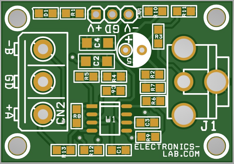
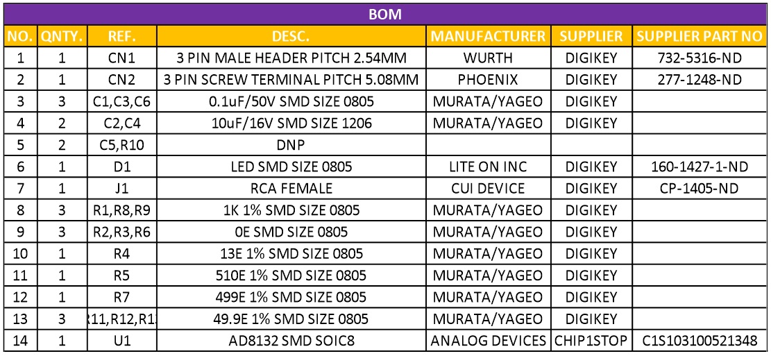
Parts List
| NO. | QNTY. | REF. | DESC. | MANUFACTURER | SUPPLIER | PART NO |
|---|---|---|---|---|---|---|
| 1 | 1 | CN1 | 3 PIN MALE HEADER PITCH 2.54MM | WURTH | DIGIKEY | 732-5316-ND |
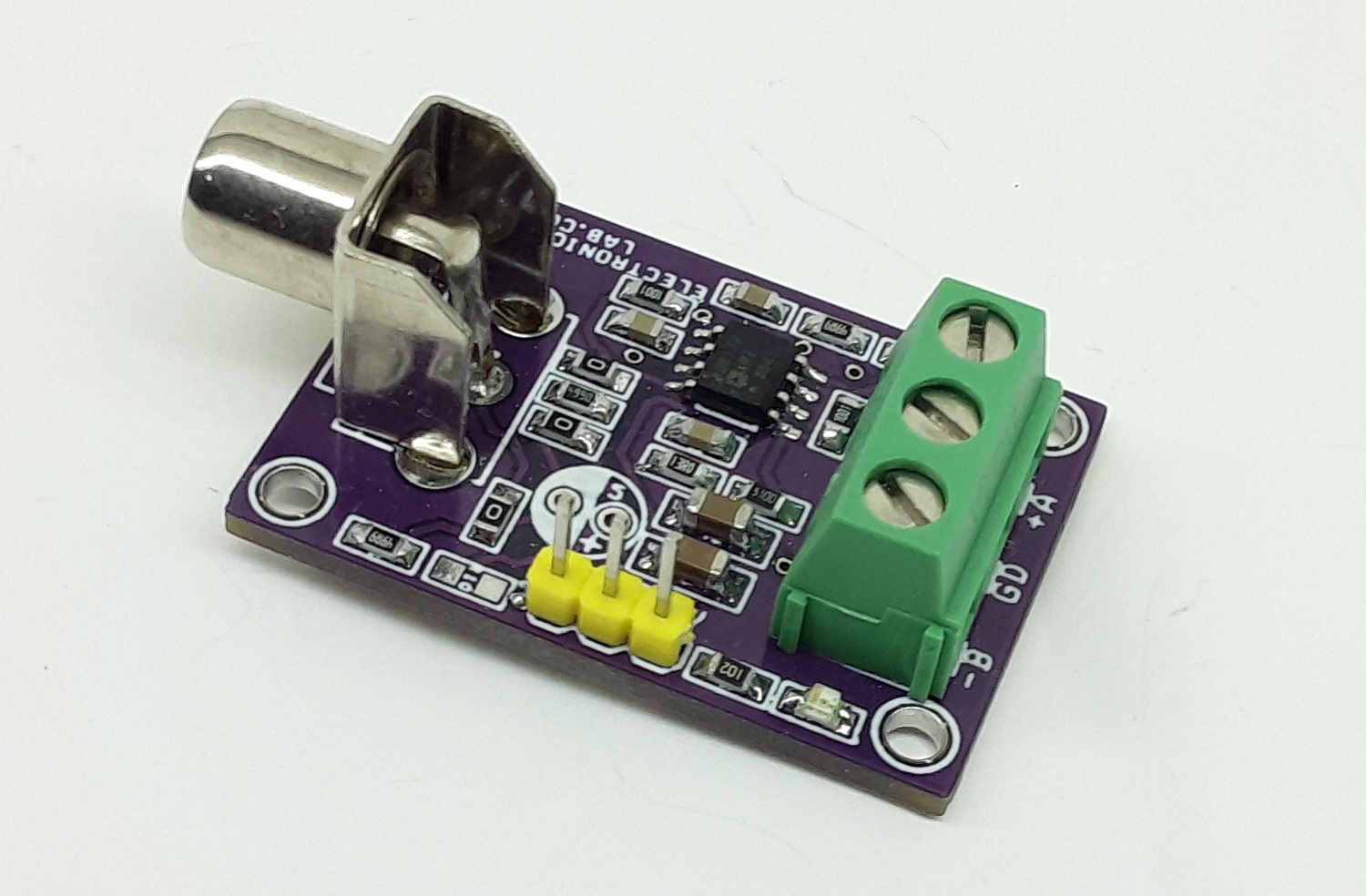
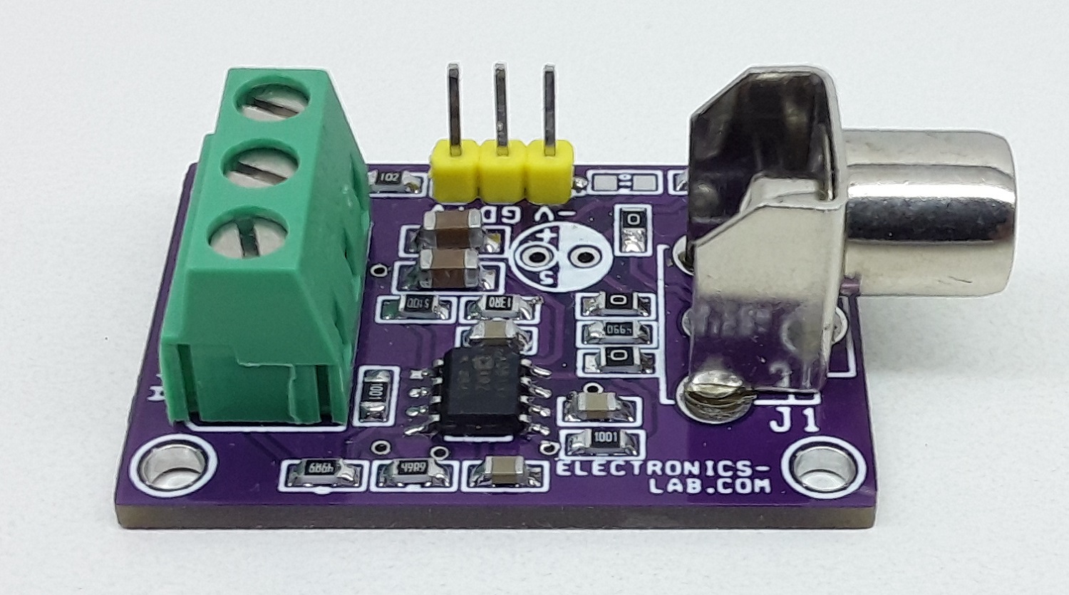
| 2 | 1 | CN2 | 3 PIN SCREW TERMINAL PITCH 5.08MM | PHOENIX | DIGIKEY | 277-1248-ND |
| 3 | 3 | C1,C3,C6 | 0.1uF/50V SMD SIZE 0805 | MURATA/YAGEO | DIGIKEY | |
| 4 | 2 | C2,C4 | 10uF/16V SMD SIZE 1206 | MURATA/YAGEO | DIGIKEY | |
| 5 | 2 | C5,R10 | DNP | |||
| 6 | 1 | D1 | LED SMD SIZE 0805 | LITE ON INC | DIGIKEY | 160-1427-1-ND |
| 7 | 1 | J1 | RCA FEMALE | CUI DEVICE | DIGIKEY | CP-1405-ND |
| 8 | 3 | R1,R8,R9 | 1K 1% SMD SIZE 0805 | MURATA/YAGEO | DIGIKEY | |
| 9 | 3 | R2,R3,R6 | 0E SMD SIZE 0805 | MURATA/YAGEO | DIGIKEY | |
| 10 | 1 | R4 | 13E 1% SMD SIZE 0805 | MURATA/YAGEO | DIGIKEY | |
| 11 | 1 | R5 | 510E 1% SMD SIZE 0805 | MURATA/YAGEO | DIGIKEY | |
| 12 | 1 | R7 | 499E 1% SMD SIZE 0805 | MURATA/YAGEO | DIGIKEY | |
| 13 | 3 | R11,R12,R13 | 49.9E 1% SMD SIZE 0805 | MURATA/YAGEO | DIGIKEY | |
| 14 | 1 | U1 | AD8132 SMD SOIC8 | ANALOG DEVICES | CHIP1STOP | C1S103100521348 |
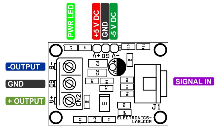
Connections
Pairing Connection
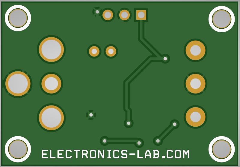
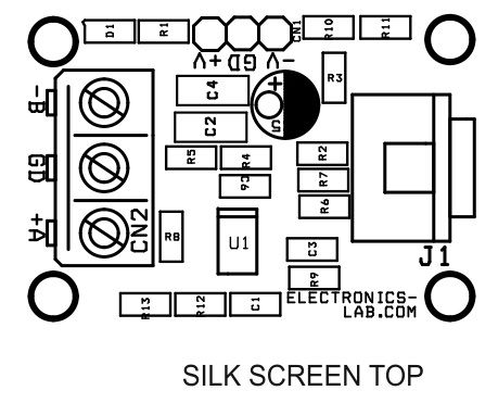
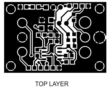
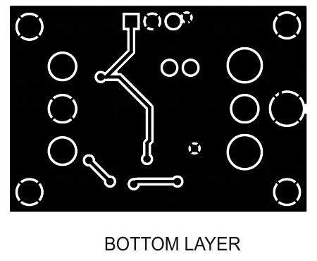
Gerber View
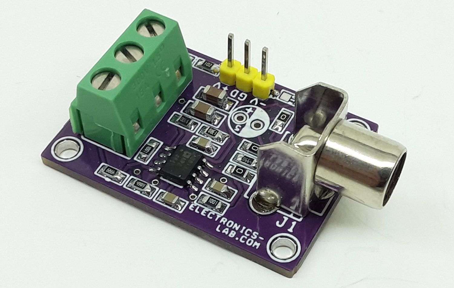
Photos

Video
AD8132 Datasheet
PCB


")

