
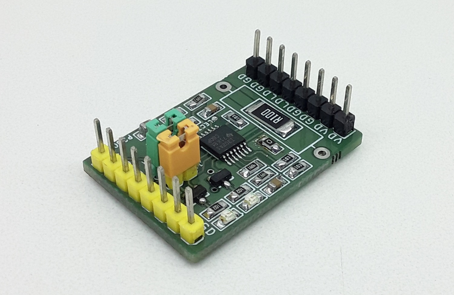
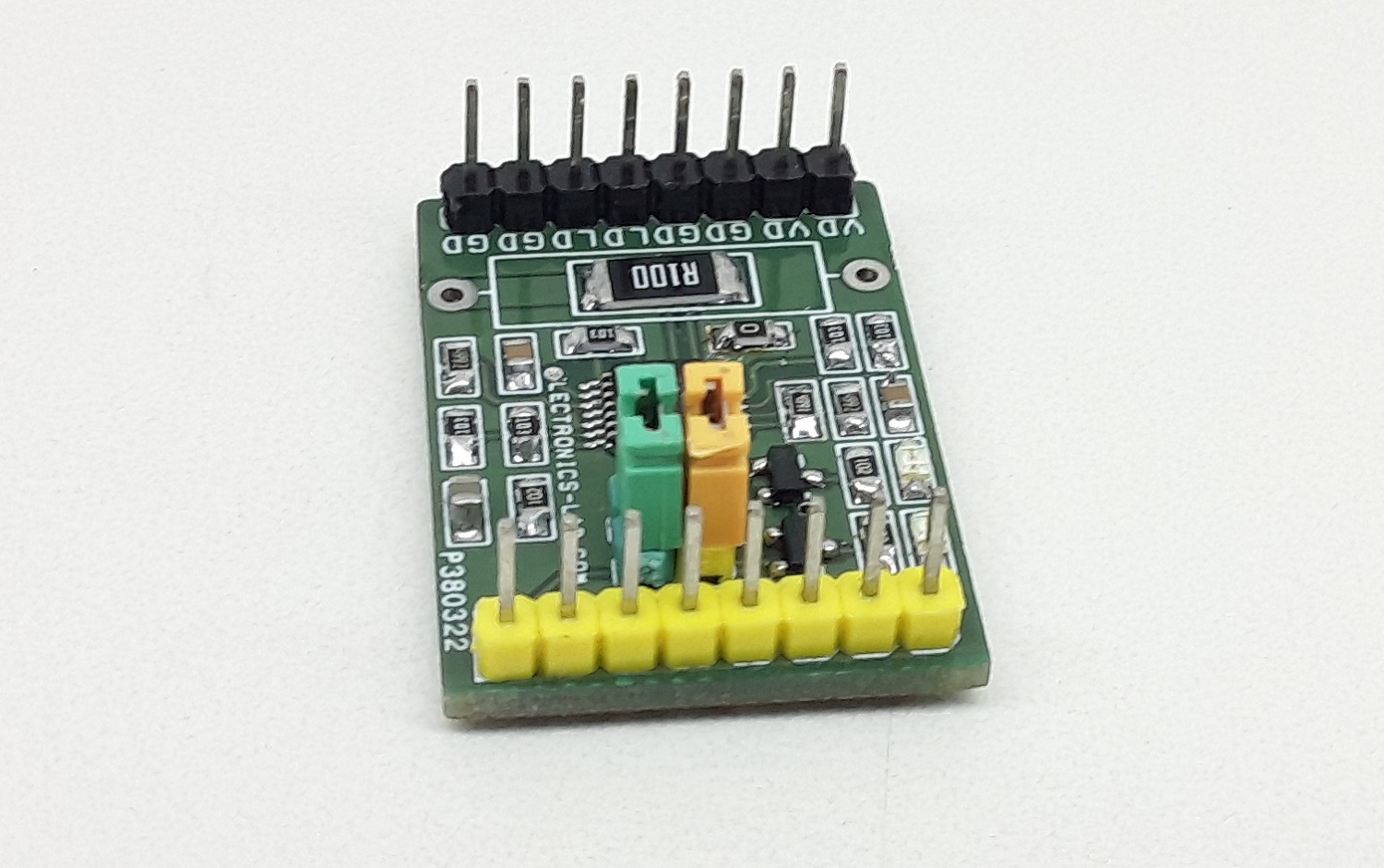
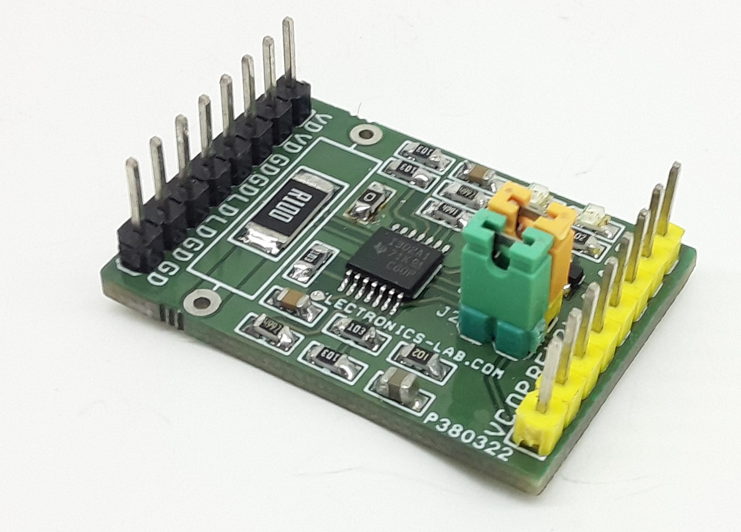
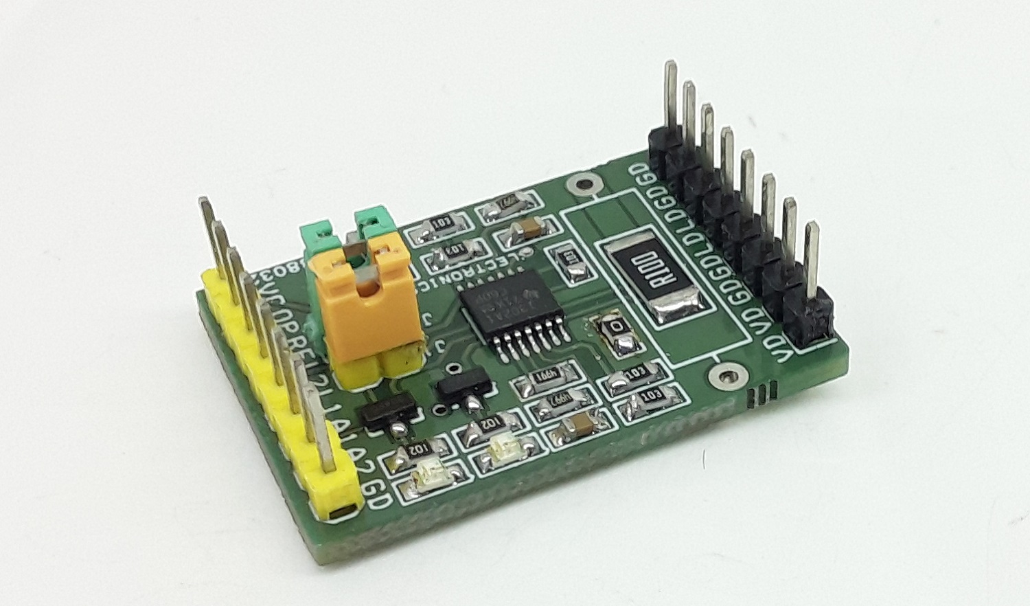
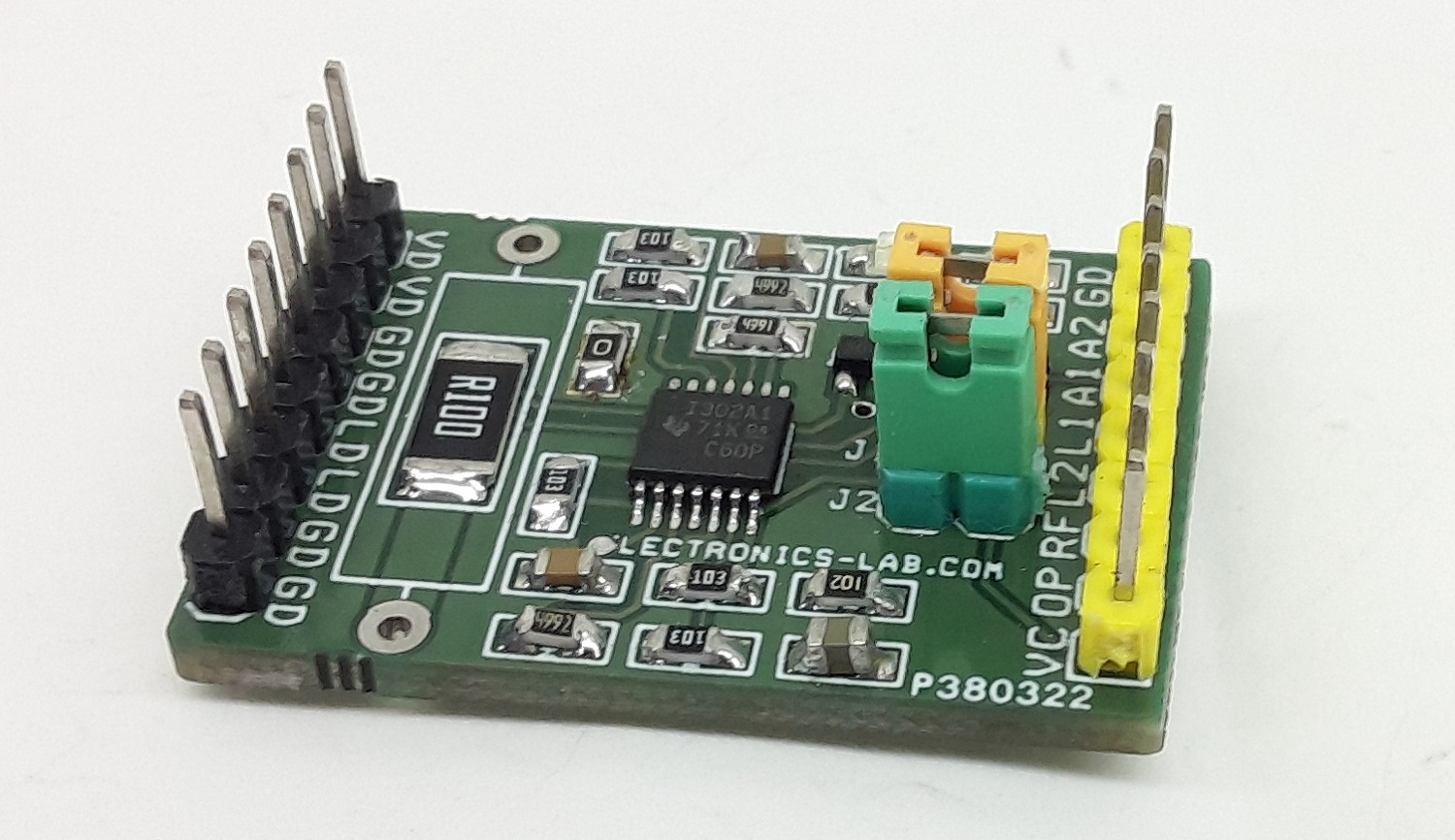
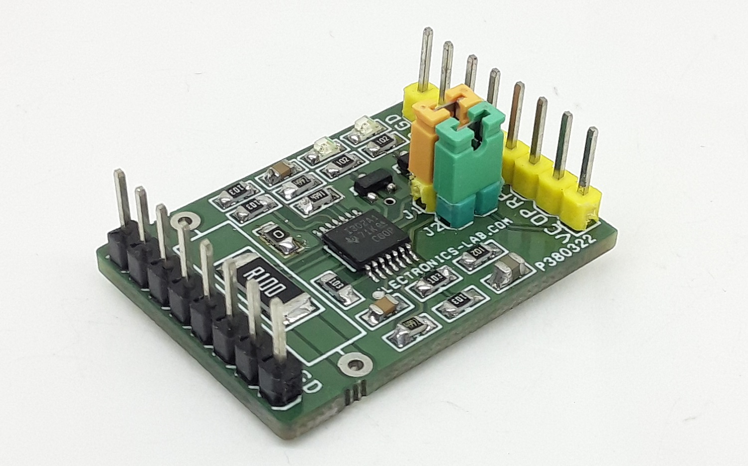
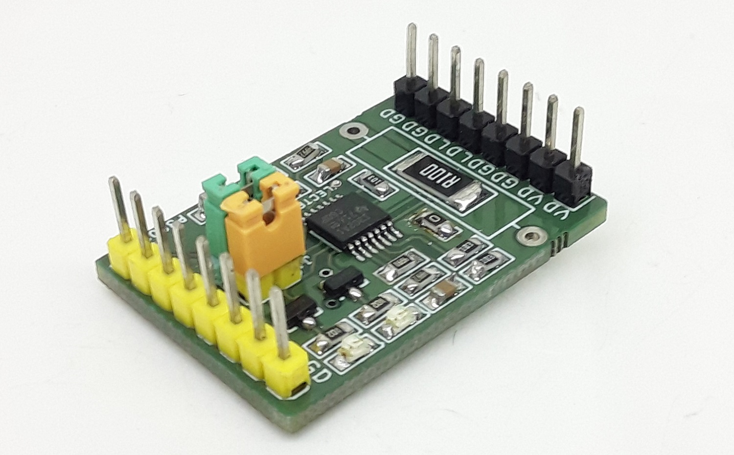
Current-Sense Amplifier with Dual Over Current Level Monitor & Alert Output
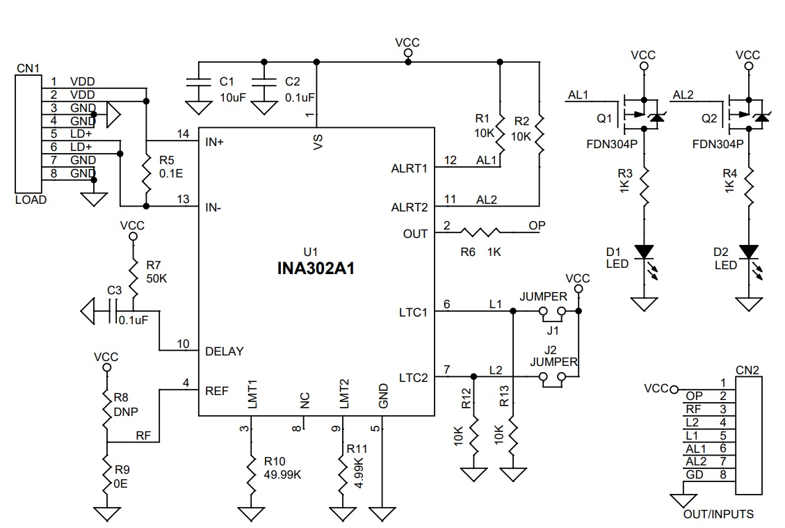
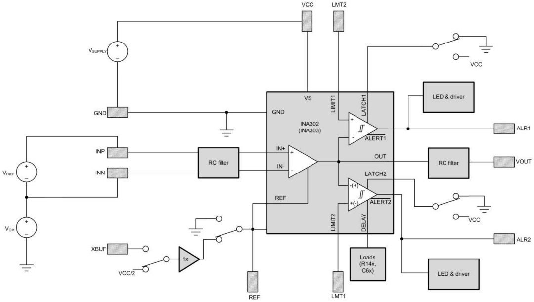
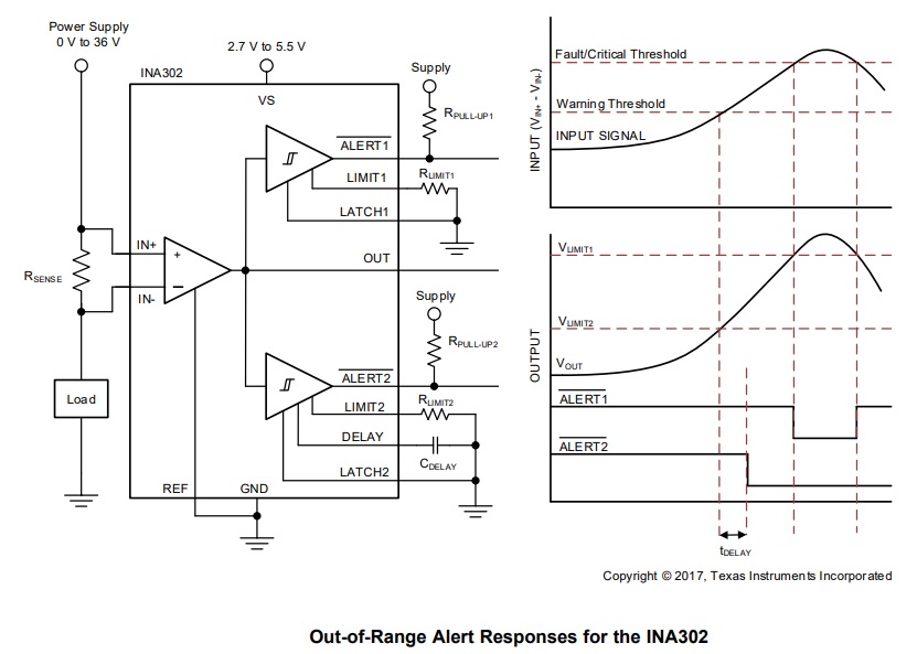
The project presented here is a high common-mode current sense amplifier with two high-speed comparators to detect out-of-range current conditions. The comparators are configured to detect and respond to dual over current conditions. These devices feature an adjustable limit threshold range for each comparator set using an external limit-setting resistor. Limit 1 Resistor is R10 and Limit 2 Resistor is R11. The board measures differential voltage signals on common-mode voltages that can vary from 0 V up to +36 V, independent of the supply.
The project is built using an INA302A1 chip which has a gain of 20V/V. The board can also be used with INA302A2 which has a gain of 50V/V or INA302A3 with a gain of 100V/V.
The open-drain alert outputs are configured to operate in either a transparent mode (output status follows the input state) or in a latched mode (alert output is cleared when the latch is reset). Jumpers J1 and J2 are provided to select this option. The alert response time for comparator 1 is under 1 µs, and the alert response for comparator 2 is set through an external capacitor ranging from 2 µs to 10 s.
- Limit 1 = R10
- Limit 2 = R11
- Current Measurements Range (By changing Shunt resistor Value) or Chip INA302A1, INA302A2, INA302A3
- Delay Time for Alert 1 and Alert 2 using resistor R7 and C3
- Bidirectional Current Sense, by applying a reference voltage to Pin 3 of CN2 or Installing Resistor R8 and R9
Features
- Supply 5V DC @ 20mA
- Input Signal Range 0 to 36V DC
- Input Current Range 0 to 2Amps
- Alert 1 and Alert 2 Dual Current Level TTL Outputs
- Alert 1 and Alert 2 Dual Current Level LED Indicator
- Delay Settings Between Alert 1 and Alert 2
- Current Sense Amplifier Voltage Output 0 to 4V
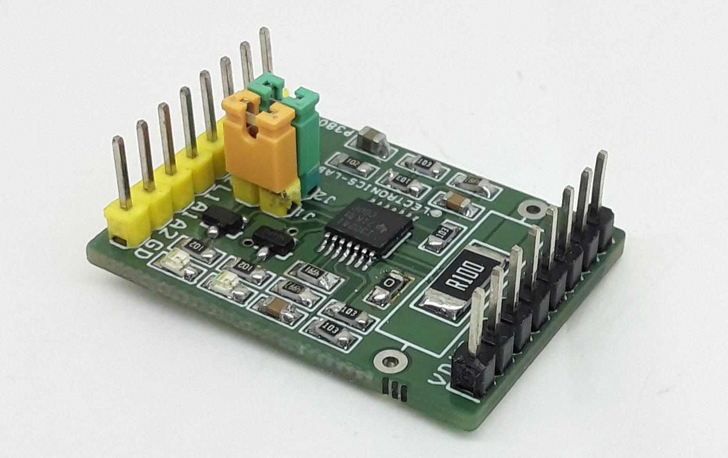
- Latch or Transparent Mode Selection Jumpers J1 and J2
- Alert2 LED On @ 200mA and Alert 1 LED On @ 2Amps Load
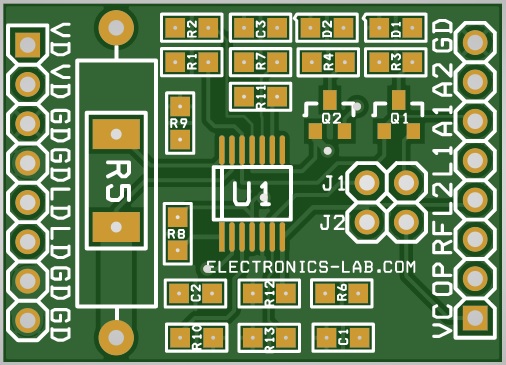
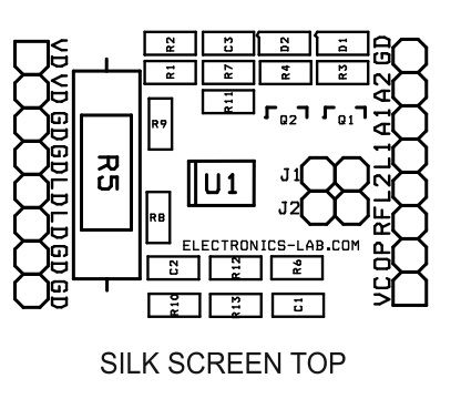
- PCB Dimensions 32.10 x 23.13 mm
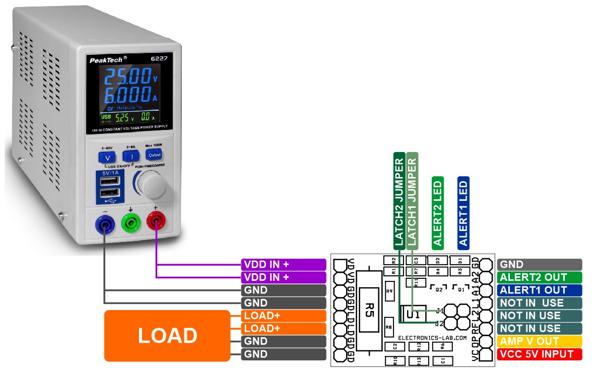
Connector CN1
- Pin1 + DC Input
- Pin2 + DC Input
- Pin3 GND
- Pin4 GND
- Pin5 Load +
- Pin6 Load +
- Pin7 GND
- Pin8 GND
Connector CN2
- Pin1 VCC 5V Power Supply Input
- Pin2 OP Current Sense Amplifier Voltage Output 0 to 4V
- Pin3 Not in Use (Reference Voltage Input)
- Pin4 Latch 2 No Use
- Pin5 Latch 3 No Use
- Pin6 Alert1 Normally High, Goes Low When Load Current = 2Amps
- Pin7 Alert2 Normally High, Goes Low When Load Current = 200mA
Limit Inputs: – Limit 1 = R10, Limit 2 = R11
The project includes onboard resistors that set the voltages at LIMIT1 and LIMIT2 to about 4 V and 400 mV, respectively.
Latch Inputs Latch 1 and Latch 2
Jumpers J1 and J2 are provided to select the transparent mode or latched operation. Default transparent mode is selected, and latched operation can be enabled by closing Jumpers J1 and J2.
Amplifier Output (0 to 4V)
The output of the internal current sense amplifier is accessible through the VOUT (OP) Pin 2 of connector CN2
ALERT1 and ALERT2 Outputs
The ALERT1 and ALERT2 pins are accessible through the Pin6 and Pin 7 of Connector CN2 labeled ALR1 and ALR2, respectively. For gross testing, users can also monitor the states of the ALERT pins using the corresponding LED-D1 and LED-D2 indicators provided on the PCB.
Signal Inputs
Input Signal Range 0 to 36V and Current sensing Range 2Amps.
Delay Input
The DELAY pin of the INA302A1 is a high-impedance node and highly susceptible to noise pickup. For this reason, all routing to the DELAY pin has been kept as short as possible. Resistor R7 and C3 allow users to control the propagation delay of the ALERT2 signal. C3 is intended for installing a load capacitor to GND. Note that the ALERT2 delay increases with load capacitance on the DELAY pin, R7 is a pull-up load resistor to VCC and helps minimize the ALERT2 delay. Installing a 50-kΩ to 100-kΩ resistor at R7 is recommended for minimal delay. Using values below 50 kΩ increases the supply current without yielding any significant reduction in the ALERT2 delay.
Schematic
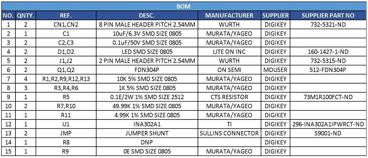
Parts List
| NO. | QNTY. | REF. | DESC. | MANUFACTURER | SUPPLIER | PART NO |
|---|---|---|---|---|---|---|
| 1 | 2 | CN1,CN2 | 8 PIN MALE HEADER PITCH 2.54MM | WURTH | DIGIKEY | 732-5321-ND |
| 2 | 1 | C1 | 10uF/6.3V SMD SIZE 0805 | MURATA/YAGEO | DIGIKEY | |
| 3 | 2 | C2,C3 | 0.1uF/50V SMD SIZE 0805 | MURATA/YAGEO | DIGIKEY | |
| 4 | 2 | D1,D2 | LED SMD SIZE 0805 | LITE ON INC | DIGIKEY | 160-1427-1-ND |
| 5 | 2 | J1,J2 | 2 PIN MALE HEADER PITCH 2.54MM | WURTH | DIGIKEY | 732-5315-ND |
| 6 | 2 | Q1,Q2 | FDN304P | ON SEMI | MOUSER | 512-FDN304P |
| 7 | 4 | R1,R2,R9,R12,R13 | 10K 5% SMD SIZE 0805 | MURATA/YAGEO | DIGIKEY | |
| 8 | 3 | R3,R4,R6 | 1K 5% SMD SIZE 0805 | MURATA/YAGEO | DIGIKEY | |
| 9 | 1 | R5 | 0.1E/2W 1% SMD SIZE 2512 | CTS RESISTOR | DIGIKEY | 73M1R100FCT-ND |
| 10 | 2 | R7,R10 | 49.99K 1% SMD SIZE 0805 | MURATA/YAGEO | DIGIKEY | |
| 11 | 1 | R11 | 4.99K 1% SMD SIZE 0805 | MURATA/YAGEO | DIGIKEY | |
| 12 | 1 | U1 | INA302A1 | TI | DIGIKEY | 296-INA302A1IPWRCT-ND |
| 13 | 2 | JMP | JUMPER SHUNT | SULLINS CONNECTOR | DIGIKEY | S9001-ND |
| 14 | 1 | R8 | DNP | DIGIKEY | ||
| 15 | 1 | R9 | 0E SMD SIZE 0805 | MURATA/YAGEO | DIGIKEY |
Connections
Reference Circuit
Block Diagram
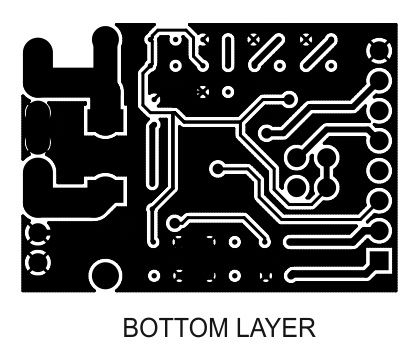
Gerber View
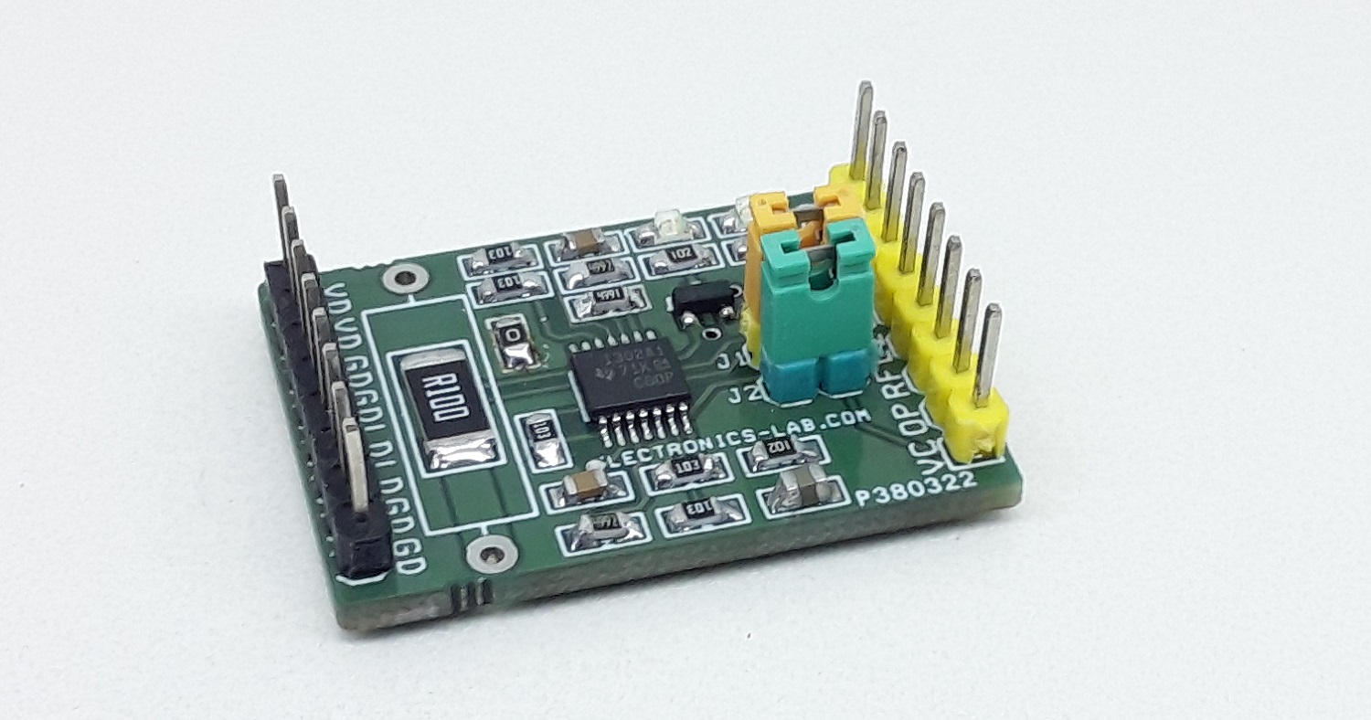
Photos
Video
INA302 Datasheet
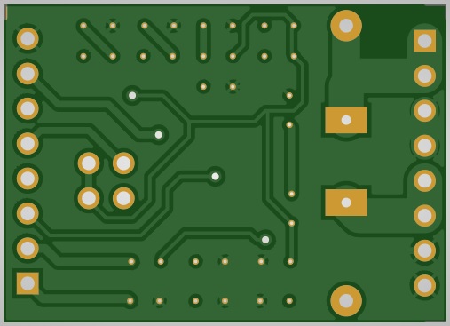
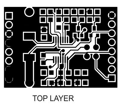
PCB