Dual-Output (Step-Up/Step-Down) DC-DC Converter via Shared Inductor Loop

CHINH NGUYEN

Jun 24, 2026
2
Joined
Jun 24, 2026
Messages
2
Logic Architecture:

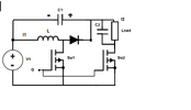
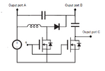
  1. Synchronous Rectification: and operate in perfect synchronicity, sharing the same gate drive signal ().
  2. Energy-Sharing Bridge (): Instead of separating the Buck and Boost stages, acts as a dynamic energy-recycling bridge. It holds the differential voltage to supply the step-down output, while maintains the traditional step-up output.
  3. Cross-Regulation Management: Utilizing a switch to toggle the Feedback (FB) signal allows the module to operate in a '2-in-1' mode. It dynamically stabilizes the primary critical load while allowing the dependent branch to adapt flexibly.
Why this is a positive breakthrough: Traditional dual-output converters require either two separate magnetic components (two inductors) or complex multi-winding transformers. This design achieves bidirectional energy cross-coupling using only one single inductor (), heavily reducing system footprint, cost, and component stress while retaining high functional flexibility.
 

Attachments

  • Screenshot (258).png
    Screenshot (258).png
    39.1 KB · Views: 4

AnalogKid

Jun 10, 2015
3,047
Joined
Jun 10, 2015
Messages
3,047
Why are you using p-channel FETs?

I see only one output.

Why is C1 connected to the positive supply rather than GND. Both are zero-ohm voltage sources.

Please post the gate drive waveform, with voltages.

ak
 

CHINH NGUYEN

Jun 24, 2026
2
Joined
Jun 24, 2026
Messages
2
Why are you using p-channel FETs?

I see only one output.

Why is C1 connected to the positive supply rather than GND. Both are zero-ohm voltage sources.

Please post the gate drive waveform, with voltages.

ak
Dear community,

To prevent any confusion and to provide a comprehensive view of this topology, I have updated the main schematic in 'Screenshot (276).png' with corrected MOSFET body diode symbols.

Additionally, I would like to supplement the technical details regarding the multi-port voltage generation and switching parameters:

1. Multi-Port Voltage Definitions:

  • Buck Output Voltage: Measured between Port A and Port B.
  • Boost Output Voltage: Measured between Port B and Port C.
2. Energy Transfer & Dynamic Cross-Coupling Mechanism:

  • The Role of C1 (Floating Buck Source): In every PWM switching cycle, when the MOSFETs turn OFF, the inductor L releases its stored energy (flyback EMF) through the diode. This energy is captured directly by C1, establishing a stable secondary voltage source VC1 that powers the buck path.
  • The Role of C2 (Boost Accumulator): The total power capability at the output is a hybrid combination: the baseline energy from the primary source VIN plus the dynamically recycled energy from VC1. This combined potential creates the elevated voltage VC2 across C2, which effectively powers the boost path.
3. Switching Control Parameters:

  • The control signal applied to the shared Gate terminal (G) is a standard PWM signal.
  • Duty Cycle range:0% to 92%.
  • Switching Frequency fsw): Designed to operate around 50 kHz or higher, depending on the dynamic switching characteristics of the chosen semiconductor components.
This structured multi-port approach turns a single-inductor configuration into a versatile power hub. I welcome your thoughts and look forward to seeing your updated simulation models based on these exact port definitions!
 

Attachments

  • Screenshot (276).png
    Screenshot (276).png
    10 KB · Views: 3
Top