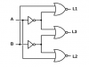
When delving into digital design, instead of relying on 'inspirational creativity' for a solution, one should learn the most common digital design procedures that will always guarantee a correct solution. These are: Truth Table, Karnaugh Map, & NAND/NOR gate implementation. I have attached a PDF which shows how to use these procedures to solve this problem and implement the solution with NOR gates.

The use of the Truth Table and Karnaugh Map are well-documented through Google. While this particular LED project is almost too simple to bother with a formal design procedure (no K-map minimization was even necessary), it would have prevented the mistake of the extraneous OR gate. Implementing the design as shown with NOR gates relies on the use of negative logic, i.e. realizing that an OR gate with negated inputs is the same as an AND gate with negated output (NAND) while an AND gate with negated inputs is the same as an OR gate with negated output (NOR). So inversion circles are selectively added to a pure logic diagram to achieve a NAND/NOR design. Two inversion circles may be added to any logic signal line while an existing inversion may be moved from one end of the signal line to the other (a negated logic variable may be shifted to invert a gate input). Negative logic may not be very intuitive but the procedure tends to not be error prone. Give it a try, you will like it.
 So this is my first Digital Logic Circuit and basically what it does is it turns on a LED depending on the decimal value of the 2-bit input. EX. 00 = 0 so no LED's are on, 01 = 1 so the 1st LED is turned on etc. I just wanted to see how I did any positive feedback would be greatly appreciated.