Question about layout of a PCB

Chengjun Li

Oct 21, 2014
84
Joined
Oct 21, 2014
Messages
84
Hi all,

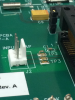
I have a chip used to measure small capacitance(aF to pF). Below is its evaluation board.
upload_2015-8-14_14-25-19.png
The area inside the red box is where I have question with. It is basically a connect lead used to connect to the capacitors being measured.
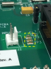
A magnified version
upload_2015-8-14_14-30-44.png upload_2015-8-14_14-39-6.png
I have two questions:
1. Why the background color on the PCB is not as dark as other area?
2. What is the thing in the yellow box?

Thanks.
 

Attachments

  • upload_2015-8-14_14-27-9.png
    upload_2015-8-14_14-27-9.png
    163 KB · Views: 75
  • upload_2015-8-14_14-30-34.png
    upload_2015-8-14_14-30-34.png
    162.9 KB · Views: 81

garublador

Oct 14, 2014
111
Joined
Oct 14, 2014
Messages
111
1. The darker part is where there is a copper fill (probably some sort of ground) and the lighter part is where there is no fill. If you were to scrape away the solder mask (the green stuff) in the lighter areas you'd find fiberglass under it. If you were to scrape away the solder mask in the darker areas you'd find copper.

2. They look like little metal loops that you can use to easily connect a probe to. They allow you to easily hook a probe on to those points and see what's happening on some sort of test equipment like an oscilloscope or something.
 

Martaine2005

May 12, 2015
5,277
Joined
May 12, 2015
Messages
5,277
And just to add to the above post, the reference designator TP is a test point as garublador suggested.

Martin
 

Chengjun Li

Oct 21, 2014
84
Joined
Oct 21, 2014
Messages
84
1. The darker part is where there is a copper fill (probably some sort of ground) and the lighter part is where there is no fill. If you were to scrape away the solder mask (the green stuff) in the lighter areas you'd find fiberglass under it. If you were to scrape away the solder mask in the darker areas you'd find copper.

2. They look like little metal loops that you can use to easily connect a probe to. They allow you to easily hook a probe on to those points and see what's happening on some sort of test equipment like an oscilloscope or something.
The lighter area is like what you said where there is no copper fill.And it works as ground plane. But that makes me confused. Ground plane is used to reduce noise and prevent crosstalk, for measuring very small capacitance, I think ground plane is vital. But why in the evaluation board, the area where capacitor being measured stays is unfill with copper foil?
 

garublador

Oct 14, 2014
111
Joined
Oct 14, 2014
Messages
111
The lighter area is like what you said where there is no copper fill.And it works as ground plane. But that makes me confused. Ground plane is used to reduce noise and prevent crosstalk, for measuring very small capacitance, I think ground plane is vital. But why in the evaluation board, the area where capacitor being measured stays is unfill with copper foil?
My understanding is that the digital ground plane can actually be fairly noisy when looked at from a precision analog standpoint. Digital signals have fast transitions, which create noise and digital signal pins generally have pretty good noise immunity (you only have to differentiate between two, discreet levels). If you couple an analog net that needs to be super precise to a digital ground plane you risk introducing noise into your signal. So the signals used to measure the capacitor are kept far away from that ground plane and are closely coupled to their own return path.

I'm not an expert in this type of design, so anyone can feel free to correct whatever I have wrong.
 

Similar threads

R
2
Replies
26
Views
4K
RST Engineering \(jw\)
R
N
Replies
9
Views
2K
Rich Grise
R
G
Replies
4
Views
1K
Glenn Ashmore
G
Top