Altium designer schematic question

lohlk

Jul 9, 2024
2
Joined
Jul 9, 2024
Messages
2
I am still a complete beginner, but I would like to learn how to use Altium Designer. Sorry in advance for the silly questions.

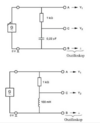
I have the following two circuits (pic no. 1) that I want to combine into one circuit and draw in Altium Designer schematic.

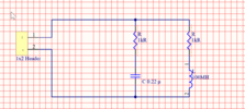
I tried to draw the mentioned circuit in Altium Designer (pic no 2). At the beginning, I created a connector header. Can this be done this way in this circuit? Do I have to change any parameters? I was thinking that if I create a connector, the generator signal can be injected through it. For the inductor, capacitor, and resistors, I changed the parameters to the respective values (capacitance, inductance, etc.) shown in pic no 1. Would my circuit approach make sense? Thank you in advance.
 

Attachments

  • Bildschirmfoto 2024-07-08 um 23.33.24.png
    Bildschirmfoto 2024-07-08 um 23.33.24.png
    245.2 KB · Views: 8
  • Bildschirmfoto 2024-07-09 um 18.43.50.png
    Bildschirmfoto 2024-07-09 um 18.43.50.png
    59.1 KB · Views: 8

Delta Prime

Jul 29, 2020
2,988
Joined
Jul 29, 2020
Messages
2,988
@Harald Kapp :
I would agree with you, but then we would both be wrong .
Considering rules of thumb,, basic principles, wire line conventions. These conventions
ensures that anyone looking at the schematic will immediately understand where signals pass to and from, and which lines carry signals and which carry power. So now we are getting into the realm of opinions,preferences, just like belly buttons everyone has an opinion.
My opinion is use connection dots for two or more wires .A wire in Altium is a polyline electrical design primitive that is used to form electrical connections between points on a schematic .
Lines should not cross or converge where possible . Crossing wires creates the appearance of a connection between lines.If lines join, I limit this to a maximum of three lines. More than three lines meeting at one point could be mistaken for unintentionally crossed lines. Schematic capture is the process of arranging components in schematic sheets and defining links between them.Altium doesn't care about how you arrange components into schematics. Circuit simulation packages like SPICE & PCB layout tools only care about the connections you define between pins on different components. These connections are called "nets," and schematic capture is really the task of creating a list of nets that will be reflected in the make up everything in your physical PCB layout,
 

davenn

Moderator
Sep 5, 2009
14,473
Joined
Sep 5, 2009
Messages
14,473
My opinion is use connection dots for two or more wires .

it isnt the world wide electronics convention .... change your opinions to align with what everyone else does :)

Lines should not cross or converge where possible .

on a reasonably complex circuit, that isnt going to happen

Crossing wires creates the appearance of a connection between lines.

ONLY if there is a dot showing connection


More than three lines meeting at one point could be mistaken for unintentionally crossed lines.

Again, dots will show connections, no dot, no connection
it's pretty straight forward :)

just an example of one of my drawings ......

1722034802583.png
 

Kiwi

Jan 28, 2013
505
Joined
Jan 28, 2013
Messages
505
Agree with you on this Dave.
Dots mean joins, no dots mean no joins.

I absolutely hate diagrams with those silly hoops where wires cross without connecting.
 
Top