Design Spark PCB

TroubledTech95

Apr 28, 2016
6
Joined
Apr 28, 2016
Messages
6
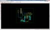
OK, so those of you who know design spark will know there is a translate to PCB option. I'm just new to it so still trying to work it all out. Every time I try to upload my schematic into it i just get all my components jumbled into the size of PCB I've chosen in a layout that is not suitable for routing and almost impossible to comprehend. Am I doing it wrong? surely to have a feature like this would be to make the PCB design/layout part more time efficient? Right now I could most definitely import the individual components and design it manually quicker.
 

Attachments

  • translate2PCB.png
    translate2PCB.png
    253.8 KB · Views: 100

(*steve*)

¡sǝpodᴉʇuɐ ǝɥʇ ɹɐǝɥd
Moderator
Jan 21, 2010
25,510
Joined
Jan 21, 2010
Messages
25,510
I generally start with rubberbands and move stuff around until it looks tidy and like it will route well before I lay down any tracks.

Can you get the software to move it to a PCB layout but not do any of the routing?
 

Arouse1973

Adam
Dec 18, 2013
5,178
Joined
Dec 18, 2013
Messages
5,178
You need to choose forward design changes option in tools not translate to PCB, use this after you have done the initial translate.
Thanks
Adam

Capture.PNG
 
Top