Hi everyone,
I'm working on a high-voltage circuit and I'd like to get some advice before I order the PCB.
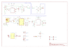
The circuit generates around 400 V at low current. The HV section uses a TLC555-based oscillator, an inductor and a switching transistor to step the voltage up from 5 V to around 400 V. There's also a separate impulse detection section.
The lower part of the schematic is the USB-C/battery charging and 5 V power supply.
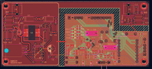
I've attached both my current schematic and PCB layout.
The stack-up is as follows:
- Signals
- Ground <- only for LV section
- Signals / Power
- Ground <- only for LV section
- 1. What's the best way to handle the ground in the HV section? Should I use a copper pour or individual traces?
- 2. How much clearance should I leave between the 400 V traces and GND copper?
- 3. Are there any particular components or nodes in the schematic that I should give extra spacing around?
- 4. Is there anything obviously wrong with having the HV section and the USB/battery circuitry on the same PCB?
- 5. Would an isolation slot or something similar be recommended anywhere?
I'd also appreciate any feedback on the schematic itself.
Thanks!


