chesschaser
- Oct 20, 2024
- 10
- Joined
- Oct 20, 2024
- Messages
- 10
Hi guys,
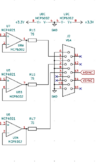
I'm making a VGA controller board for Arduino, and it looks good to me, but just want a sanity check (especially for the RP2040 section, as I have never used that before) before proceeding to PCB production.
I can't breadboard test it as the frequencies involved are too high.
How it works (or how it's SUPPOSED to work):
The Arduino SPI is nowhere NEAR fast enough for VGA pixel clock timing (25.175MHz), so I am offloading the framebuffer into a SPI SRAM (23LC1024). If MS is pulled low then REFRESH is pulsed, it signals the RP2040 to do the frame update sequence. MS (master select) selects the master the SRAM is connected to. The RP2040 will read the framebuffer and send the data over SPI to the MCP4921 DACs. The LDAC pin is pulsed low only after this is completed, so all three color channels update at once. The voltage followers are for isolation. VREF is chosen to be 1.4V so that the output of the 75 ohm series resistor forming a voltage divider with the one inside the monitor is 0.7V, scaling the analog values to 0V-0.7V, standard VGA.
The firmware on the RP2040 (manually programmed through the W25Q128JVS flash memory chip) will handle pixel clock via PLL, and HYSNC and VYSNC pulse timing). Obviously it is too slow for full resolution, so a reduced resolution will have to do.
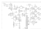
EDIT: Part of the circuit seems to be cut off, so I have added it as a second image.
Thanks in advance!!!
I'm making a VGA controller board for Arduino, and it looks good to me, but just want a sanity check (especially for the RP2040 section, as I have never used that before) before proceeding to PCB production.
I can't breadboard test it as the frequencies involved are too high.
How it works (or how it's SUPPOSED to work):
The Arduino SPI is nowhere NEAR fast enough for VGA pixel clock timing (25.175MHz), so I am offloading the framebuffer into a SPI SRAM (23LC1024). If MS is pulled low then REFRESH is pulsed, it signals the RP2040 to do the frame update sequence. MS (master select) selects the master the SRAM is connected to. The RP2040 will read the framebuffer and send the data over SPI to the MCP4921 DACs. The LDAC pin is pulsed low only after this is completed, so all three color channels update at once. The voltage followers are for isolation. VREF is chosen to be 1.4V so that the output of the 75 ohm series resistor forming a voltage divider with the one inside the monitor is 0.7V, scaling the analog values to 0V-0.7V, standard VGA.
The firmware on the RP2040 (manually programmed through the W25Q128JVS flash memory chip) will handle pixel clock via PLL, and HYSNC and VYSNC pulse timing). Obviously it is too slow for full resolution, so a reduced resolution will have to do.
EDIT: Part of the circuit seems to be cut off, so I have added it as a second image.
Thanks in advance!!!
")