Can I please get help with this?
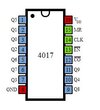
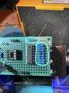
As you can see by the picture of the circuit I am building, I am connecting the resistors to the 4017 Chip. The circled resistor at the very top, is connected to Pin 9 ( I thought I would mention this, as it is not obvious from the picture).
My question is this:
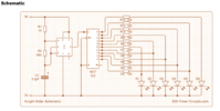
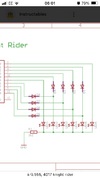
The circuit is building one of those Knight Rider police light things.
The schematic shows that a total of 10 resistors are being used (2 220 Ohms, and 8 100 Ohms. But I only have 9 resistors soldered on my board. I am obviously missing one resistor but I cannot figure out which pin on the 4017 I should connect the missing 100 Ohm resistor to.
Thank-you for your help.
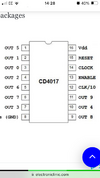
As you can see by the picture of the circuit I am building, I am connecting the resistors to the 4017 Chip. The circled resistor at the very top, is connected to Pin 9 ( I thought I would mention this, as it is not obvious from the picture).
My question is this:
The circuit is building one of those Knight Rider police light things.
The schematic shows that a total of 10 resistors are being used (2 220 Ohms, and 8 100 Ohms. But I only have 9 resistors soldered on my board. I am obviously missing one resistor but I cannot figure out which pin on the 4017 I should connect the missing 100 Ohm resistor to.
Thank-you for your help.