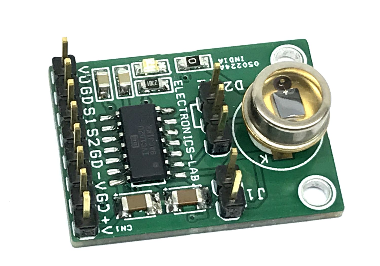
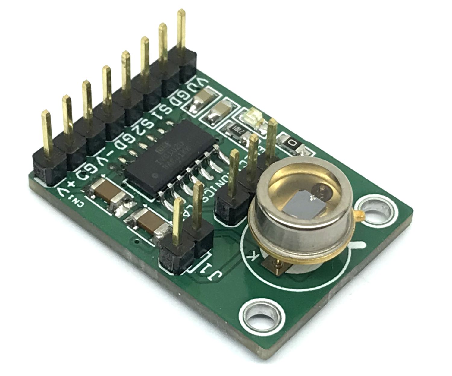
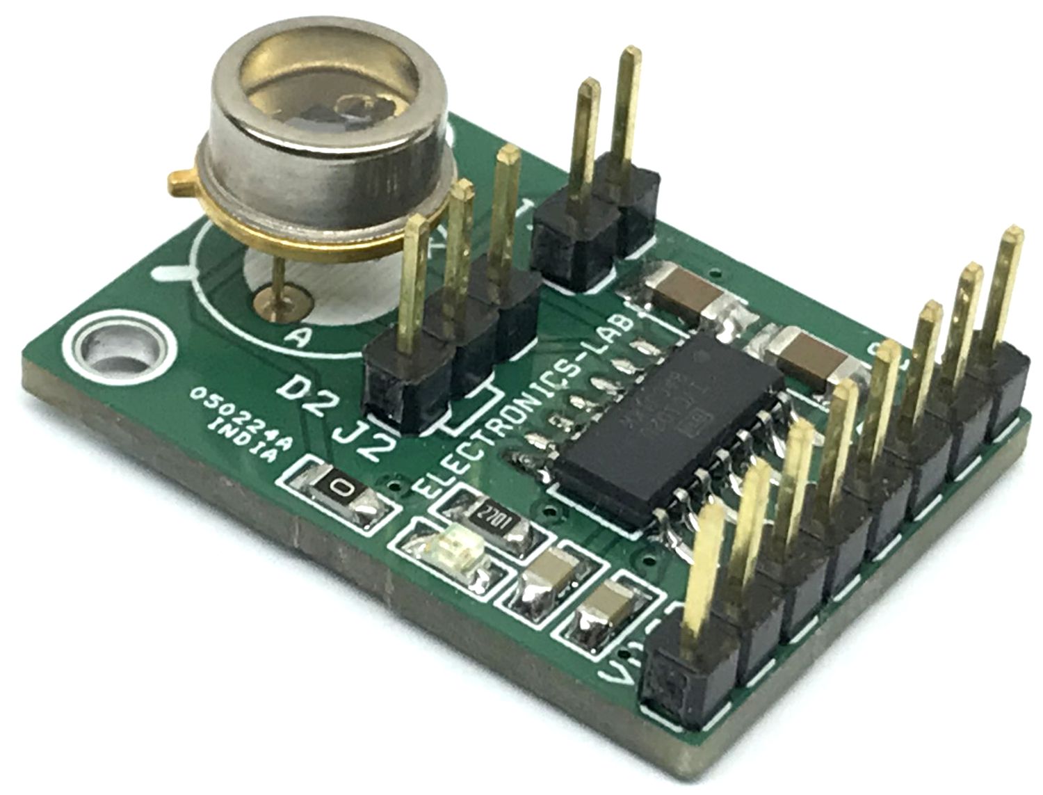
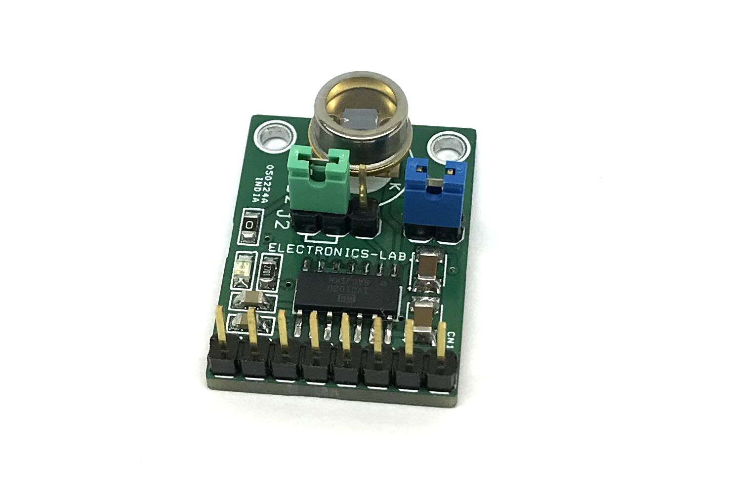
Precision Switched Integrator Transimpedance Amplifier
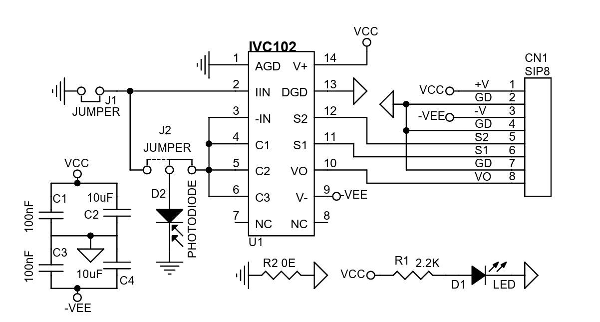
This project is based on IVC102 chip from Texas Instruments. This chip is a precision integrating amplifier with FET OPAMP, integrating capacitors, and low leakage FET switches.
This project is based on IVC102 chip from Texas Instruments. This chip is a precision integrating amplifier with FET OPAMP, integrating capacitors, and low leakage FET switches. It integrates low-level input current for a user-determined period, storing the resulting voltage on the integrating capacitor. The output voltage can be held for accurate measurement. The IVC102 provides a precision, lower-noise alternative to conventional transimpedance OPAMP circuits that require a very high-value feedback resistor. The project is ideal for amplifying low-level sensor currents from photodiodes and ionization chambers. The input signal current can be positive or negative. TTL/CMOS-compatible timing inputs control the integration period, hold, and reset functions to set the effective transimpedance gain and reset (discharge) the integrator capacitor. Jumpers are provided to configure the circuit for photodiode amplifier or ionization chamber measurement.
Features
- Power Supply +/-15V Dc
- On-Chip Integrating Capacitors
- Switch Signal TTL 5V
- Gain Programmed By Timing
- Low Input Bias Current: 750fA Max
- Low Noise
- Low Switch Charge Injection
- Fast Pulse Integration
- Low Nonlinearity: 0.005% Type
- PCB Dimensions 28.73 x 20.96 mm
- 2 x 2.5mm Mounting Holes
Applications
- Precision Low Current Measurement
- Photodiode Measurements
- Ionization Chamber Measurements
- Current/Charge-Output Sensors
- Leakage Current Measurement
Basic Reset-and-Integrate Measurement
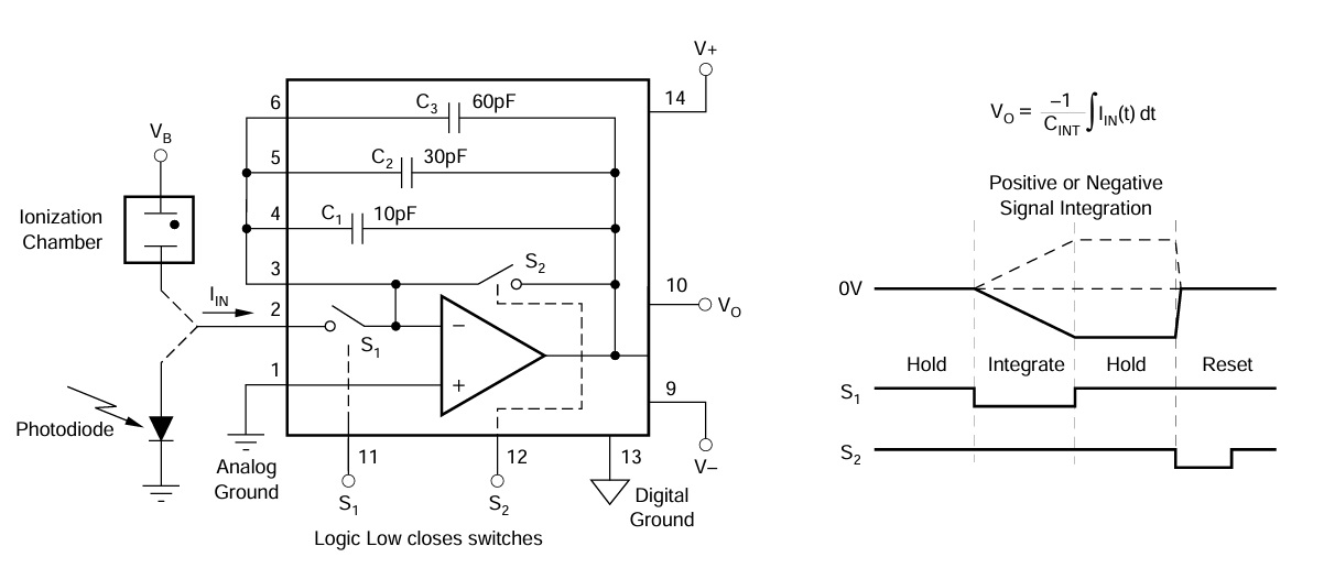
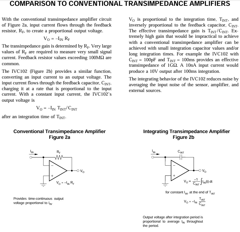
Figure 1 shows the circuit and timing for a simple reset-and integrate measurement. The input current is connected directly to the inverting input of the IVC102, pin 3. Input current is shown flowing out of pin 3, which produces a positive-going ramp at VO. Current flowing into pin 3 would produce a negative-going ramp. A measurement cycle starts by resetting the integrator output voltage to 0V by closing S2 for 10µs. Integration of the input current begins when S2 opens and the input current begins to charge CINT. VO is measured with a sampling a/d converter the end of an integration period, just prior to the next reset period. The ideal result is proportional to the average input current (or total accumulated charge). Switch S2 is again closed to reset the integrator output to 0V before the next integration period. This simple measurement arrangement is suited to many applications. There are, however, limitations to this basic approach. Input current continues to flow through S2 during the reset period. This leaves a small voltage on CINT equal to the input current times RS2, the on-resistance of S2, approximately 1.5kΩ. In addition, the offset voltage of the internal op amp and charge injection of S2 contribute to the voltage on CINT at the start of integration. Performance of this basic approach can be improved by sampling VO after the reset period at T1 and subtracting this measurement from the final sample at T2. Op amp offset voltage, charge injection effects and I•RS2 offset voltage on S2 are removed with this two-point measurement. The effective integration period is the time between the two measurements, T2-T1.
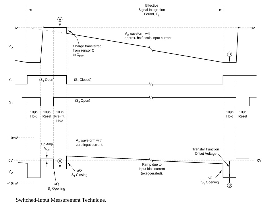
Switched-Input Measurement Technique
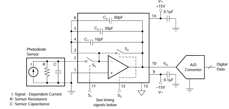
While the basic reset-and-integrate measurement arrangement in Figure 1 is satisfactory for many applications, the switched-input timing technique shown in Figure 3 has important advantages. This method can provide continuous integration of the input signal. Furthermore, it can hold the output voltage constant after integration for stable conversion (desirable for AD converter without a sample/hold). Input connections and timing are shown in Figure 3. The timing diagram, Figure 3b, shows that S1 is closed only when S2 is open. During the short period that S1 is open (30µs in this timing example), any signal current produced by the sensor will charge the sensor’s source capacitance. This charge is then transferred to CINT when S1 is closed. As a result, no charge produced by the sensor is lost and the input signal is continuously integrated. Even fast input pulses are accurately integrated.
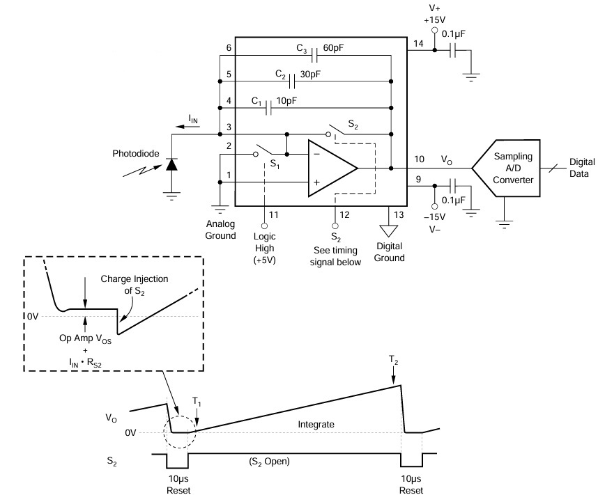
The input current, IIN, is shown as a conventional current flowing into pin 2 in this diagram but the input current could be bipolar (positive or negative). Current flowing out of pin2 would produce a positive-ramping VO. The timing sequence proceeds as follows: Reset Period The integrator is reset by closing switch S2 with S1 open. A 10µs reset time is recommended to allow the op amp to slew to 0V and settle to its final value-Integration Hold S2 is opened, holding VO constant for 10µs prior to integration. This pre-integration hold period assures that S2 is fully open before S1 is closed so that no input signal is lost. A minimum of 1µs is recommended to avoid switching overlap. The 10µs hold period shown in Figure 3b also allows an a/d converter measurement to be made at point A. The purpose of this measurement at A is discussed in the “Offset Errors” section. Integration on CINT Integration of the input current on CINT begins when S1 is closed. An immediate step output voltage change occurs at the charge that was stored on the input sensor capacitance is transferred to CINT. Although this period of charging CINT occurs only while S1 is closed, the charge transferred as S1 is closed causes the effective integration time to be equal to the complete conversion period—see Figure 3b. The integration period could range from 100µs to many minutes, depending on the input current and CINT value. While S1 is closed, IIN charges CINT, producing a negative going ramp at the integrator output voltage, VO. The output voltage at the end of integration is proportional to the average input current throughout the complete conversion cycle, including the integration period, reset and both hold periods. Hold Period Opening S1 halts integration on CINT. Approximately 5µs after S1 is opened, the output voltage is stable and can be measured (at point B). The hold period is 10µs in this example. CINT remains charged until a S2 is again closed, to reset for the next conversion cycle. In this timing example, S1 is open for a total of 30µs. During this time, signal current from the sensor charges the sensor source capacitance. Care should be used to assure that the voltage developed on the sensor does not exceed approximately 200mV during this time. The IIN terminal, pin 2, is internally clamped with diodes. If these diodes forward bias, signal current will flow to ground and will not be accurately integrated. A maximum of 333nA signal current could be accurately integrated on a 50pF sensor capacitance for 30µs before200mV would be developed on the sensor. IMAX = (50pF) (200mV)/30µs = 333nA
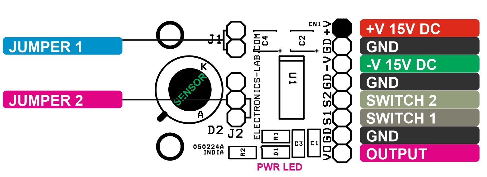
Connections
- Pin 1 = +15V DC
- Pin 2 = GND
- Pin 3 = -15V DC
- Pin 4 = GND
- Pin 5 = S2
- Pin 6 = S1
- Pin 7 = GND
- Pin 8 = Output
- Jumper J1 and J2 for Photo Diode or Ionized Chamber Selection
- D2: Photodiode, Select as per Application Requirements
- D1: Power LED
Schematic
Parts List
| NO | QNTY. | REF | DESC | MANUFACTURER | SUPPLIER | SUPPLIER PART NO |
|---|---|---|---|---|---|---|
| 1 | 1 | CN1 | 8 PIN MALE HEADER PITCH 2.54MM | WURTH | DIGIKEY | 732-5321-ND |
| 2 | 2 | C1,C3 | 100nF/50V CERAMIC SMD SIZE 0805 | YAGEO/MURATA | DIGIKEY | |
| 3 | 2 | C2,C4 | 10uF/25V CERAMIC SMD SIZE 1210 OR 1206 | YAGEO/MURATA | DIGIKEY | |
| 4 | 1 | D1 | LED SMD SIZE 0805 | OSRAM | DIGIKEY | 475-1278-1-ND |
| 5 | 1 | D2 | PHOTODIODE , AS PER APPLICATION | |||
| 6 | 2 | J2 | 3 PIN MALE HEADER PITCH 2.54MM | WURTH | DIGIKEY | 732-5316-ND |
| 7 | 1 | R1 | 2.2K 5% SMD SIZE 0805 | YAGEO/MURATA | DIGIKEY | |
| 8 | 1 | R2 | 0E 5% SMD SIZE 0805 | YAGEO/MURATA | DIGIKEY | |
| 9 | 1 | U1 | IVC102 | TI | DIGIKEY | 296-41281-1-ND |
| 10 | 1 | J1 | 2 PIN MALE HEADER PITCH 2.54MM | WURTH | DIGIKEY | 732-5315-ND |
| 11 | 1 | J1,J2 | SHUNT FOR JUMPER J1,J2 | SULINS CONNCT | DIGIKEY | S9001-ND |
Connections
Block Diagram
Application Schematic
Measurements Schematic
Gerber View
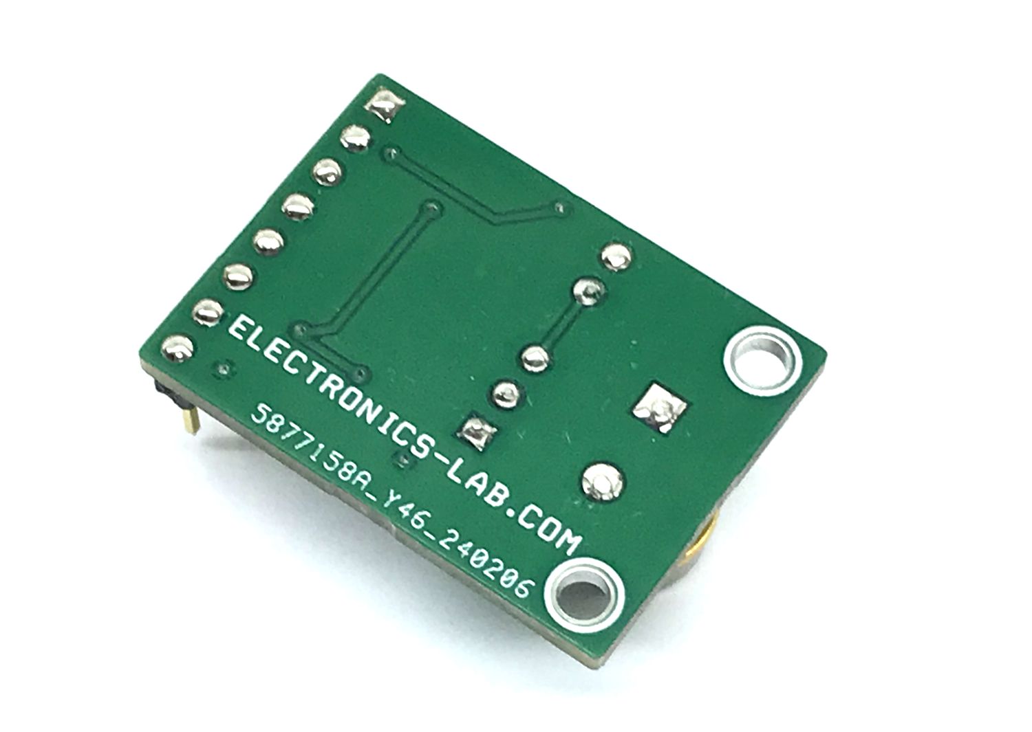
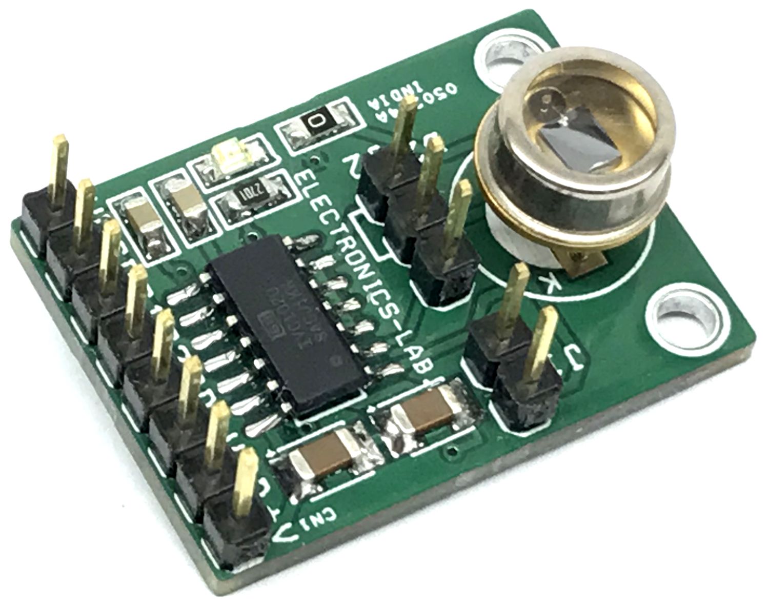
Photos