walid
-
Posts
749 -
Joined
-
Last visited
Never
Content Type
Profiles
Forums
Events
Everything posted by walid
-
Hi guru unless R3 = R4 the charge time will not = the discharge time in the circuit R3=820 and R4=1000, why not equal? thank you
-
thank you Ante
-
Hi how did u know it is 200mA, can u please explain it for me thank you
-
Hi my best guru I can't discribe my feeling, you really the MAESTRO of this great site u make the information appeared in the photo below, you make it very clear. thank u guru, I wish you all the best in the world yours walid
-
To guru thank u very very much you are good and expert man. this is a part of a circuit shown in the following link: http://www.electronics-lab.com/forum/index.php?topic=10229.0 it is an IC controlled emergency lamp with charger
-
Thank you guru, u r truly remarkable man
-
Hi Why, usually using a resistor with little resistance and high-value wattage in battery chargers circuits? why not connecting the batt directly with the source? thank you
-
Hi can you explain What R8 (1K) exactly do? is it a voltage divider?? thanks
-
Hi please look at the figure below: if as seen, the X1 secondary voltage is 6V AC, then the rectified DC voltage after the bridge and a cap (1000u/25V) filter is 6* sqrt 2 =8.49 VDC is this true, please comment. thanks
-
Hi guru I am very sorry, I did not notice it. How wonderful it for a zener non-existent My understanding is that the cap charged through only R3, but now I do not know how dischargting, or to any point, is it to pin is 6 or 7 of the 555 IC. and why he do so, what shape of the o/p pulse he want? please explain it for me.
-
Hi all In the attached file below u can find the circuit diagram of the IC controlled emergency lamp with charger my question is what the purpose of using D5 and D8, what they do in the circuit?? thanks
-
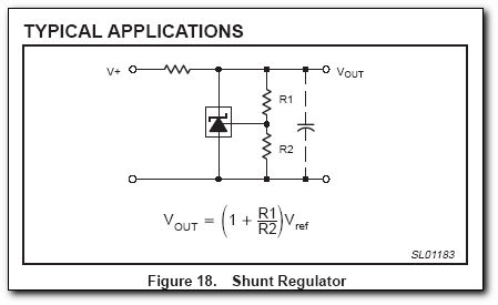
Hi I have another question about the shunt regulator 431: We Know that Vout = (1 + [R1/R2]) * Vref If I want Vout 12.5V and assume Vref = 2.5V then 12.5/2.5 = 5 that is R1/R2 =4 400K/100K = 4 4ohm/1ohm =4 ???!!!!! I read three different 431 datasheets from three different companies trying to find something about the values of that resistos, but nothing. can u please help thanks
-
Thank u guru No problem, I didn't calculate it, only I put random numbers to know the value of Vref, you are clearly mentioned in Your previous answer I got what I want Thank you once again for your attention.
-
thank you guru fore your direct and good answer, it was very good also thank for Ldanielrosa
-
Hi In its datasheets attached below, and looking to the atteched figure below, we can see that: Vout = (1 + [R1/R2]) * Vref If +V = 12v, R1 =10k, R2=2K What is Vout I cannt understand how to get Vref value please help me to solve this thanks 431-2.pdf
-
ok thank u guru
-
hi guru You did not understand me, so I'll ask the question once again : The 2N3904 transistor have the following char. from datasheet: Po = 625 mW Ic max = 200 mA VEC max = 40 V from that, if we have VCE = 5V, the max IC = 625m/5= 125 mA Now if at saturation, VCE=0.4 V, then Ic max = about 1.6 A my question now, can i use a load draw 1.5A in a swtching circuit using 2N3904 thanks
-
Suppose that You used a transistor 2N3904, in its datasheet I found that the Po = 625 mW; the power which this transistor can dissipate (in the form of heat) equal to 625 m Watt. Now, if we assume that VCE = 0.4 V at saturation, this transistor can pass to 1.5 ampere as Ic. But in the datasheet Ic max = 200mA I read from this page: http://www.kpsec.freeuk.com/trancirc.htm that: The power developed in a switching transistor is very small: In the OFF state: power = Ic × VCE, but Ic = 0, so the power is zero. In the full ON state: power = Ic × VCE, but VCE = 0 (almost), so the power is very small. can you explain to me to what value of Ic I can operate this transistor. thank you.
-
Brothers hurt, the most important stage in the Computer power supply is the input stage
-
point me please
-
Hi often have some friends with their remote control to to repair it. This requires that you have the examiner Cristal to ensure the validity of this piece. In the past, I was immediately replaced them with new, but I know I need to examine the crystal. Searched in the internet and I found this circuit and structure but did not work, therefore decided to understand it very well that to succeed when structure the next time. I deleted the 56p cap because I do not need to watch the freq. I know that the first transistor worked as oscillator and the o/p sig rectified by the two diodes to the final stage which will be ON if the first stage oscillate. My questions: 1) is the 1st stage is colpitts osc. 2) How the value of frequency depends on crystal? 3)Why 680p and 150p caps, What if others these values?
-
Hi guru thank you for fast reply In my country, there is a puplic open market, they sold scrap, half a telephone 1/4 radio part of vedio recorder..etec every month, i go to this market any by some boards i have this 1/2 phone, it is senao, it is at least 10 km long. After this discussion with you, now i don't want to take parts of this phone and reconstruct it to a Tx and Rx. but you open my eyes to new things merit to look at and discuss i gained till this moment some important information about narrow and widebands and can imagine now how modulation process takes place (sorry for bad grammar) Why manufatures go to a higher freqs, is it better? this is a good information and from it i can diduce that mine is transmit at 1.7MHz AM and receive at 27MHz FM. what the range of freqs of Citizen's Band? at this time I'm near to finish the drawing of the o/p section starting from the antenna, the filter is very complex series and parallel combinations of caps and air coils (look at the last photo), i'll put it here to discuss it with u to learn new things. thank you guru
-
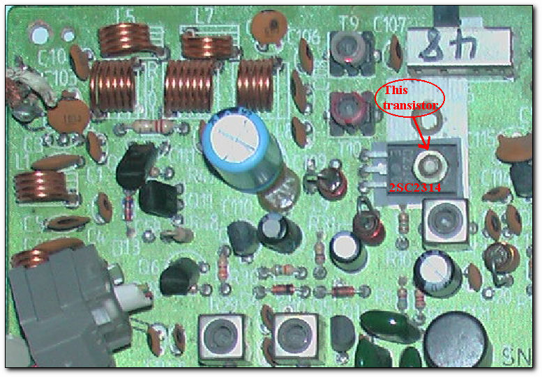
Hi guru Ok, I understand that you have never looked inside one before and u have never seen a schematic of a narrowband dual conversion FM receiver circuit before. But also I know that u still have the ability to help me. I need you theory information to help me in my trip inside that cordless phone. I the fiq below, I’ll concentrate on the 2sc2314 transistor, in its datasheets I read: 27MHz CB Transceiver Driver Applications 1) What the meaning of CB? 2) Is 27MHz mean that the operating freq of both TX and Rx is 27MHz? 3) What you understand from using that transistor? Thank you 2sc2314.pdf
-
Hi guru As you know if u click on th followin image it will become bigger http://www.electronics-lab.com/forum/index.php?action=dlattach;topic=9699.0;id=6451;image can you please tell me where the TX to draw it thank you
-
Hi guru dont worry I'll draw the schematic and discuss it with you. I can do it, u help me, we can do it. now i'll draw the Rx (3359) and related parts and put it here, then u tell me where the TX part I see the two LM567CN, i know they are for tone detection I'll draw all pars in sequance and discuss them with you guru I want to work hard and I need you help what u say??? yours Walid