All Activity
- Yesterday
-

Unusual Transformer Windings Ratio Problem. Tech comments Needed!
russwr replied to russwr's topic in Power Electronics
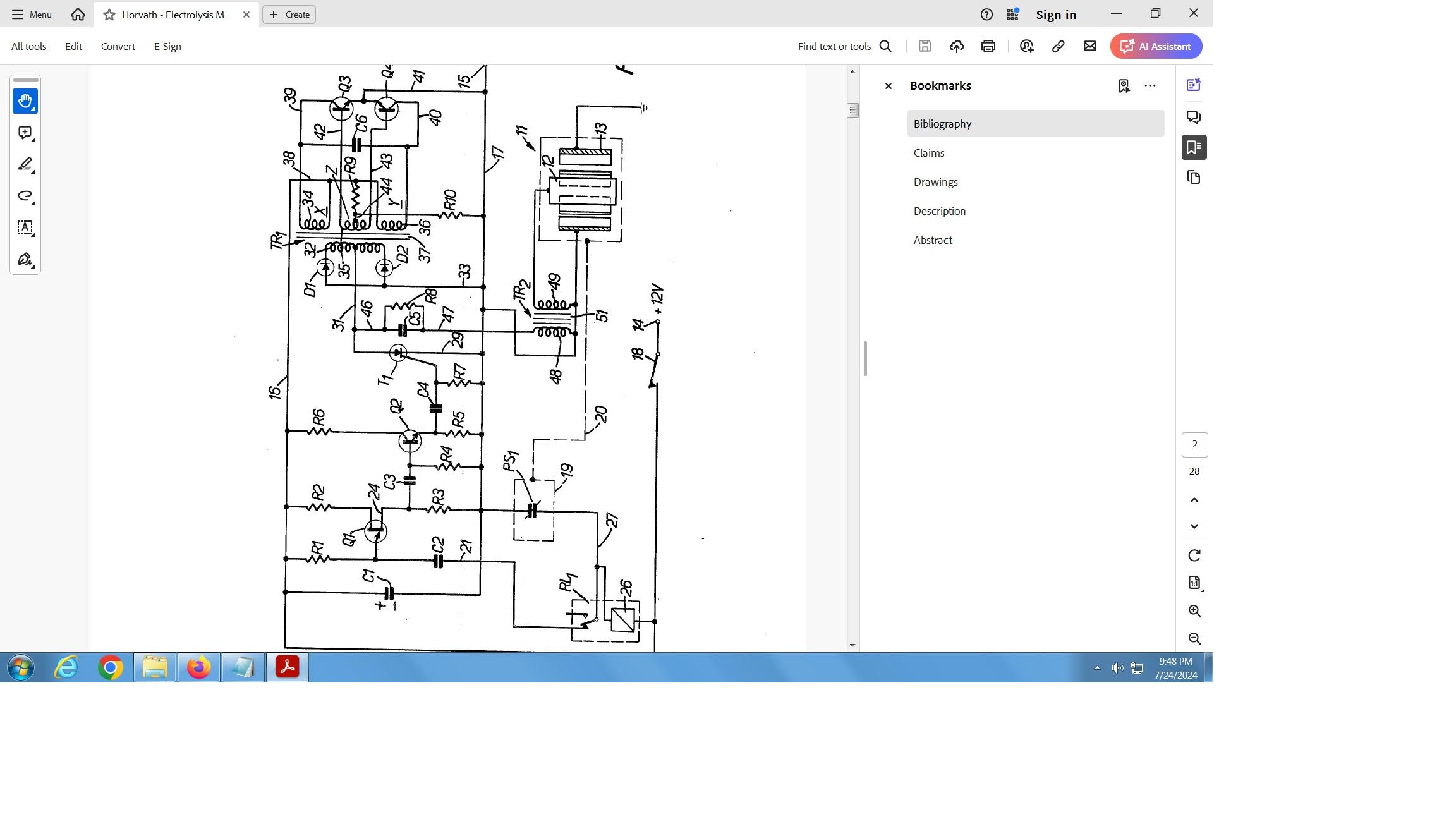
I said the device was used for improved efficiency of electrolysis of water to hydrogen. The Patent said so. The complete explanation STEP BY STEP is in the Patent write up with a parts list.. The 2 transformers in circuit were hand assembled as pertinent only for that circuit. The Inverter is NOT similar to the old style methodology, due to the type of rectification used. You did not read / study US Patent 3980053 for free Internet on line, to grasp the significance of this invention. A firm does not expend $5000 for attorney fees to process Patent application without substantial merit. Engineer Horvath's first 2 patents related were similar but differed as to final output of either low voltage or high voltage. His last Patent referred to Magnetron radiation tube in water cell center delivering sufficient hydrogen fuel. The final take on this overall, is that several special parts as described are not really necessary, and are there just to deter people from trying to duplicate the system. His self running car at 40 amps power draw, was public demonstrated several times and in local newspaper New Zealand. -
 RATAN HEMBRAM joined the community
 -
 Ericson Colina joined the community
 -
 Lazario Peepin joined the community
 - Last week
-
 Nathan ONeil OBrien changed their profile photo
 -
 Ivy Michael joined the community
 -
I studied US Patent 3980053 vigorously years ago. I typed 2 pages of proof reading errors made by the Patent Examiners. Doing a recent review of my findings, the ratio of windings is lastly, still a problem. The main circuit is just a beefed up capacitor discharge ignition at 600watts, and used for electrolysis, instead of low wattage unit for running a common ignition coil. There is an "inherent" built in lowered efficiency set up ,designed in by Horvath, on purpose. The schematic electrical hook up in the Patent is to be able to use heavy amps as a final , without using a heat/energy wasting rectifier at 200 pulse amps at 600 watts. This brilliant small section of circuit solves the energy waste problem, but the step down windings ratio was incorrectly stated in Patent. With 300 volts injected by the cap into primary inductance, there seems to be a 270v loss to get to 30volts , and then a 10: 1 ratio, for final 3 volts DC. I then assumed there was a mistake as it should be 100: 1 ratio. But then again, that CANNOT BE RIGHT SINCE THERE IS AN INHERENT EFFICIENCY LOSS BUILT IN. The beginning power supply Inverter is high frequency 10,000 cycles. The 1st transformer for the Inverter is FERRITE CORE, which is normally designed for that frequency. The second following transformer using the discharge cap and ratio has low grade, low frequency iron laminations core. This speciality is for the designed in output pulse called critical positive voltage damped wave form, as a degraded final signal. (No heat loss from a 200 amp diode.) The core produces heat which is used to heat the water. The question being presented here is, is it true then, because of the larger winding core loss of low frequency laminations on high frequency, that the REAL final winding ratio would be changed to approx 70 : 1 to be able to still get the required 3 volts as final?? I understand that Patents don't reveal exacting details, and the typed Patent should say 100:1,- they said 10:1 and are both wrong. Instructions for the small CDI units for car or small engine ignition say that the high frequency unit is hooked to the regular auto ignition coil. Ignition coils are all called autotransformers with 3 terminals. The interior CORES ARE ALL low frequency iron laminations. Maybe I am reading too much into this, as it is common for cdi to use the iron lamination cores. What we didn't know was, the output pulse is POSITIVE DC VOLTAGE. In The Patent, Capacitor discharges 22 amps pulse at 300v DC into primary coil 185microhenries. The ratio primary to secondary side changes current to 200amps pulse at 10,000 times a second.This then creates sufficient hydrogen fuel along with the other increases in efficiency for water cell. The engines then, run on water from tank. That particular ratio was 1 to 10 for higher amps. to cell. The amount of current injected relates to quantity of fuel gases evolved. What about the voltage reduction ratio??? 300 to 3 is not 10 to 1 ratio. Is there really a 270v loss in the transfer?? Something is going on here! If 300v changes to 3 volts at 100 to 1 ratio, then 22amps would chance to 2200amps. (The 200 amps sounds more reasonable.) Your comments needed #1 Horvath Patents Allowed Engine To Run On Water Improved Electrolysis Efficiency 09-13-2023, 05:03 PM I studied the Horvath Patents for a long time,way back, and understand the circuits. A duplication does not need a new cast carburetor and machined spoked electrodes as in Patent. The Electrical circuit is just a beefed up capacitor discharge ignition for MAIN POWER, with improved efficiency electrolysis for hydrogen and oxygen at 40 amps, 450 watts battery draw. The spark plugs are changed to zero ohms racing type or just get Champion brand with same reach threads and remove resistor from top, and replace with bit of #12 copper wire segment. The gases flow from water safety can to a "spud in jet" as fitting on side of old 1 barrel carburetor at the venturi point. This beveled copper tube + farrow seal cap was also used on small engines on propane conversion without the expensive type kit purchase. Read Patent 3980053, then I can answer you about how it works. A 1994 Chevy Geo Metro 3 cylinder engine with fuel system injector replaced with a used, single barrel Carter carburetor would suffice. You make an aluminum plate adapter. It has a distributor that can be adjusted for timing. The Patent transformer core size was given, so as I had enlarged photo on copy machine to get size of other parts.Substitutes can be used when ordering parts as long as the necessary design systems are included. The on time of current pulses was 42 microseconds out of 100.. 1 / F = Period of frequency.10khz = 100 microseconds time. The duty cycle of oscillator was .006. (.6usec/100usec) 22 amps cap discharge = 300V DC X square root of 1microfarad / 185 microhenries coil of TR2 primary.. Frequency of pulses to SCR was 10,000 cycles. Tr1 FERRITE type transformer charges up the capacitor to 300v AC. Diodes added for full wave DC..Main capacitor HAS TO BE ONLY polypropylene 1MFD AT 1000 VOLTS DC type as LOW esr. The 22 was amps into primary of TR2. The secondary side was 10:1 ratio. The fast switch SCR is only the high frequency type like a GE model 35 amp. The reverse pulse on the primary side circuit of TR2 shuts off SCR inbetween pulses automatically. The 200A cell pulses creates more Hydrogen with the aid of magnetic field.The TR2 secondary uses NO DIODE RECTIFIER as the pulses ARE called "critical positive wave" with core as laminations, for the high frequency , instead of ferrite. This causes degraded pulse wave as positive DC. Get laminations from take apart microwave old transformer. You would build NARROW rectangle box of high temperature Gray pvc plates. . Two SS magnetic type plates and metal strips to add to each for spokes. The large Alnico or small multiple STRONG Neodymium magnets get taped to outside of box. N + S on opposite sides box. The cover gets holes for various brass fittings. Cut out rectangle rubber seal and drilled + tapped holes for cover screws.Magnetic Field is between the electrode strip gaps under water. The Oxygen and Hydrogen gaseous bubbles rise up and transfer to special brass wool type fast one way valve before entering the safety water can. Water cell should use baking soda with distilled water, so as no cleaning of container minerals build up. The Metro engine compartment is LARGE and has plenty room to work. Engine could also be put on engine stand, but you would need the Bell housing because the starter motor mounts there.. The car called Geo Metro XFI model with 3cyl did get the highest gas mileage of any car- 52MPG. In Canada it was called the Firefly. Don't forget to buy test meters such as LCR tester. The Analog type face + needle multimeters will measure volts at high frequency, not digital. Float valve attached to cover and small DC water pump, white plastic plug in breadboard for oscillator, ect, you get the idea. I have the sheet of proof reading corrections from poor Patent examiner mistakes. Last edited by russwr; 09-13-2023, 05:34 PM. #2 Today, 11:34 AM I studied US Patent 3980053 vigorously years ago. I typed 2 pages of proof reading errors made by the Patent Examiners. Doing a recent review of my findings, the ratio of windings is lastly, still a problem. The main circuit is just a beefed up capacitor discharge ignition at 600watts, and used for electrolysis, instead of low wattage unit for running a common ignition coil. There is an "inherent" built in lowered efficiency set up ,designed in by Horvath, on purpose. The schematic electrical hook up in the Patent is to be able to use heavy amps as a final , without using a heat/energy wasting rectifier at 200 pulse amps at 600 watts. This brilliant small section of circuit solves the energy waste problem, but the step down windings ratio was incorrectly stated in Patent. With 300 volts injected by the cap into primary inductance, there seems to be a 270v loss to get to 30volts , and then a 10: 1 ratio, for final 3 volts DC. I then assumed there was a mistake as it should be 100: 1 ratio. But then again, that CANNOT BE RIGHT SINCE THERE IS AN INHERENT EFFICIENCY LOSS BUILT IN. The beginning power supply Inverter is high frequency 10,000 cycles. The 1st transformer for the Inverter is FERRITE CORE, which is normally designed for that frequency. The second following transformer using the discharge cap and ratio has low grade, low frequency iron laminations core. This speciality is for the designed in output pulse called critical positive voltage damped wave form, as a degraded final signal. (No heat loss from a 200 amp diode.) The core produces heat which is used to heat the water. The question being presented here is, is it true then, because of the larger winding core loss of low frequency laminations on high frequency, that the REAL final winding ratio would be changed to approx 70 : 1 to be able to still get the required 3 volts as final?? I understand that Patents don't reveal exacting details, and the typed Patent should say 100:1,- they said 10:1 and are both wrong. Instructions for the small CDI units for car or small engine ignition say that the high frequency unit is hooked to the regular auto ignition coil. Ignition coils are all called autotransformers with 3 terminals. The interior CORES ARE ALL low frequency iron laminations. Maybe I am reading too much into this, as it is common for cdi to use the iron lamination cores. What we didn't know was, the output pulse is POSITIVE DC VOLTAGE. In The Patent, Capacitor discharges 22 amps pulse at 300v DC into primary coil 185microhenries. The ratio primary to secondary side changes current to 200amps pulse at 10,000 times a second.This then creates sufficient hydrogen fuel along with the other increases in efficiency for water cell. The engines then, run on water from tank. That particular ratio was 1 to 10 for higher amps. to cell. The amount of current injected relates to quantity of fuel gases evolved. What about the voltage reduction ratio??? 300 to 3 is not 10 to 1 ratio. Is there really a 270v loss in the transfer?? Something is going on here! If 300v changes to 3 volts at 100 to 1 ratio, then 22amps would chance to 2200amps. (The 200 amps sounds more reasonable.) (Or just maybe, the LAST actual proof reading error in the US Patent, was the ORIGINALLY WRONG FINAL VOLTAGE, AS It should be 30 volts PULSE DC!) 10 to one Ratio for both voltage 300v down to 30v and current up from 22A to 200A. (The 200 amps sounds more reasonable.) Your comments needed!

-
I'm having a lot of trouble finding a user's manual for my old Daewoo CTS2090 CRT TV. S/N BUS210209112090


-
 1393 joined the community
 -
 The TS-M1030D is a compact Bluetooth Low Energy (BLE) Bluetooth module, featuring a Bluetooth 5.0 chip and support for BLE4.2 and BLE+SPP dual-mode protocols. It also supports AT commands, allowing users to modify parameters such as serial port baud rate and device name. Additionally, the data control module’s I/O ports can be directly accessed via an app for flexible and straightforward operation. This module offers outstanding stability, ultra-low cost, minimal power consumption, and high receiving sensitivity. Model No.: TS-M1030D Features Bluetooth Version: BLE 4.2+SPP 3.0 Frequency Band: 2.402GHz-2.480GHz ISM band TX Power: -20dBm~+4dBm Receive Sensitivity: -97dBm Air Rate: 250Kbps/1Mbps/2Mbps Antenna: PCB Onboard Advise Range: 80m Memory: 160KB FLASH+20KB RAM Size: 17*13*1.5mm Pin/GPIO: 21/16 Power Supply: 1.8~3.6V Operating Temperature: -40℃~+85℃ Peripheral Interface: UART/SPI/I2C/ADC Serial Transparent Transmission Rate: BLE 4KB/s, SPP 16KB/s Applications Smart home Location tracking Intelligent educational equipment Measurement and monitoring system Industrial sensors and controls Medical equipment monitoring and wireless control
 -
 In order to fully meet the growing demand in the AIoT market for high-performance, high-computing-power, and low-power main controllers, Forlinx Embedded has recently launched the FET3576-C System on Module, designed based on the Rockchip RK3576 processor. It features excellent image and video processing capabilities, a rich array of interfaces and expansion options, low power consumption, and a wide range of application scenarios. This article delves into the distinctive benefits of the Forlinx Embedded FET3576-C SoM from four key aspects. Advantages: 6TOPS computing power NPU, enabling AI applications Forlinx Embedded FET3576-C SoM has a built-in 6TOPS super arithmetic NPU with excellent deep learning processing capability. It supports INT4/ INT8/ INT16/ FP16/ BF16/ TF32 operation. It supports dual-core working together or independently so that it can flexibly allocate computational resources according to the needs when dealing with complex deep learning tasks. It can also maintain high efficiency and stability when dealing with multiple deep-learning tasks. FET3576-C SoM also supports TensorFlow, Caffe, Tflite, Pytorch, Onnx NN, Android NN and other deep learning frameworks. Developers can easily deploy existing deep learning models to the SoM and conduct rapid development and optimization. This broad compatibility not only lowers the development threshold, but also accelerates the promotion and adoption of deep learning applications. Advantages: Firewall achieves true hardware resource isolation The FET3576-C SoM with RK3576 processor supports RK Firewall technology, ensuring hardware resource isolation for access management between host devices, peripherals, and memory areas. Access Control Policy - RK Firewall allows configuring policies to control which devices or system components access hardware resources. It includes IP address filtering, port control, and specific application access permissions. Combined with the AMP system, it efficiently manages access policies for diverse systems. Hardware Resource Mapping and Monitoring - RK Firewall maps the hardware resources in the system, including memory areas, I/O devices, and network interfaces. By monitoring access to these resources, RK Firewall can track in real-time which devices or components are attempting to access specific resources. Access Control Decision - When a device or component attempts to access hardware resources, RK Firewall will evaluate the access against predefined access control policies. If the access request complies with the policy requirements, access will be granted; otherwise, it will be denied. Isolation Enforcement - For hardware resources identified as requiring isolation, RK Firewall will implement isolation measures to ensure that they can only be accessed by authorized devices or components. In summary, RK Firewall achieves effective isolation and management of hardware resources by setting access control policies, monitoring hardware resource access, performing permission checks, and implementing isolation measures. These measures not only enhance system security but also ensure system stability and reliability. Advantages: Ultra clear display + AI intelligent repair With its powerful multimedia processing capability, FET3576-C SoM provides users with excellent visual experience. It supports H.264/H.265 codecs for smooth HD video playback in various scenarios, while offering five display interfaces (HDMI/eDP, MIPI DSI, Parallel, EBC, DP) to ensure compatibility with diverse devices. FET3576-C SoM notably supports triple-screen display functionality, enabling simultaneous display of different content on three screens, significantly enhancing multitasking efficiency. In addition, its 4K @ 120Hz ultra-clear display and super-resolution function not only brings excellent picture quality enjoyment, but also intelligently repairs blurred images, improves video frame rate, and brings users a clearer and smoother visual experience. Advantage: FlexBus new parallel bus interface FET3576-C of Forlinx Embedded offers a wide range of connectivity and transmission options with its excellent interface design and flexible parallel bus technology. The FlexBus interface on the SoM is particularly noteworthy due to its high flexibility and scalability, allowing it to emulate irregular or standard protocols to accommodate a variety of complex communication needs. FlexBus supports parallel transmission of 2/4/8/16bits of data, enabling a significant increase in the data transfer rate, while the clock frequency of up to 100MHz further ensures the high efficiency and stability of data transmission. In addition to the FlexBus interface, the FET3576-C SoM integrates a variety of bus transfer interfaces, including DSMC, CAN-FD, PCIe2.1, SATA3.0, USB3.2, SAI, I2C, I3C and UART. These interfaces not only enriches the SoM's application scenarios but also enhances its compatibility with other devices and systems. It is easy to see that with the excellent advantages of high computing power NPU, RK Firewall, powerful multimedia processing capability and FlexBus interface, Forlinx Embedded FET3576-C SoM will become a strong player in the field of embedded hardware. Whether you are developing edge AI applications or in pursuit of high-performance, high-quality hardware devices, the Folinx Embedded FET3576-C SoM is an unmissable choice for you.
 -
 Alexander Drache changed their profile photo
 -
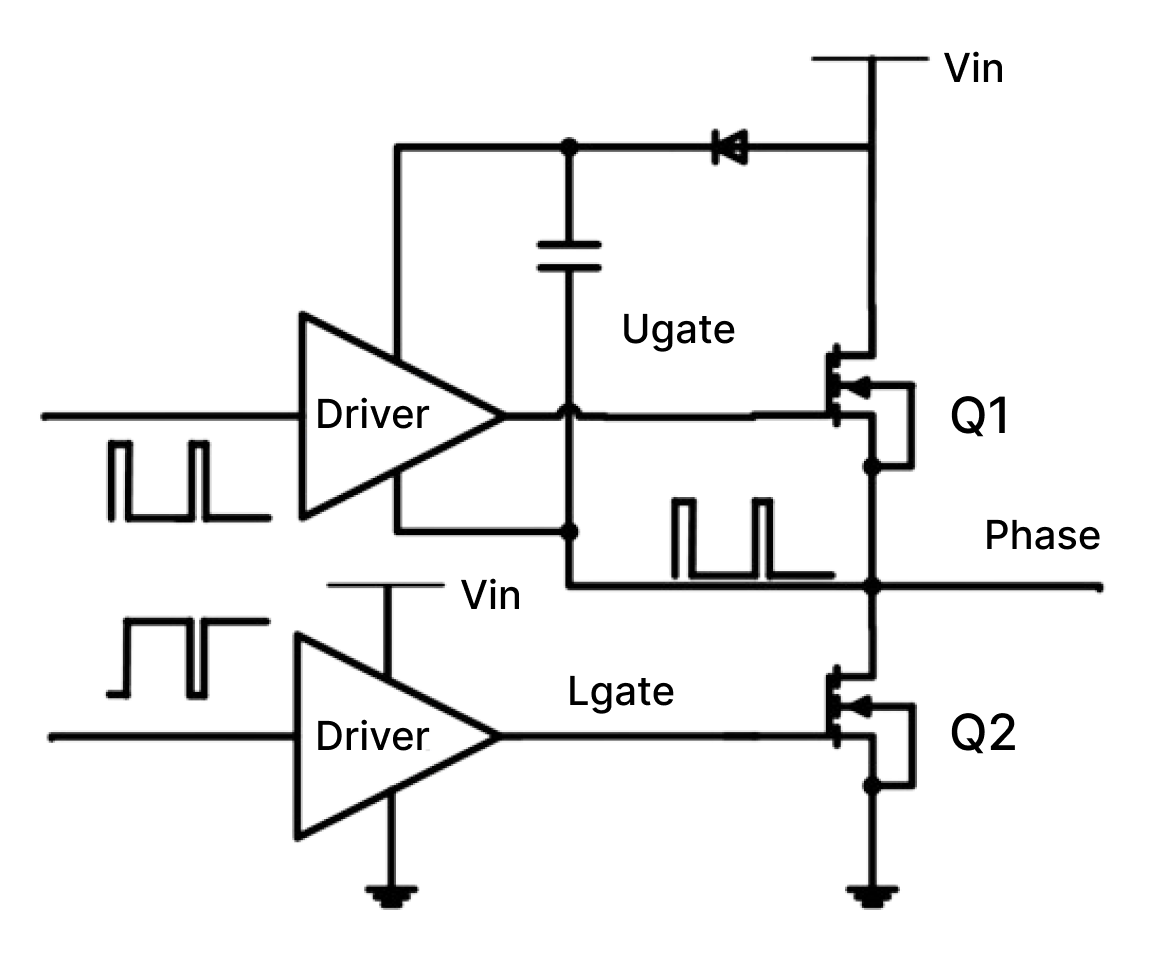
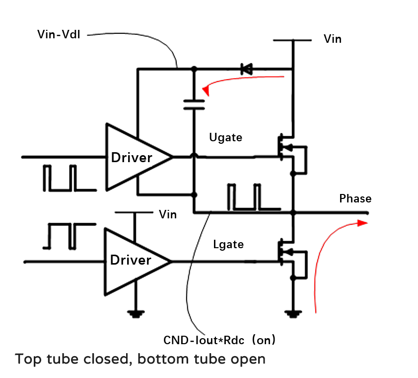
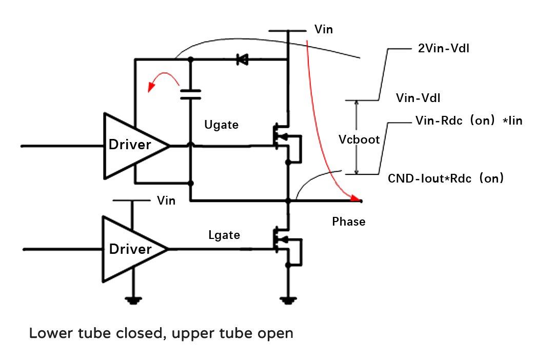
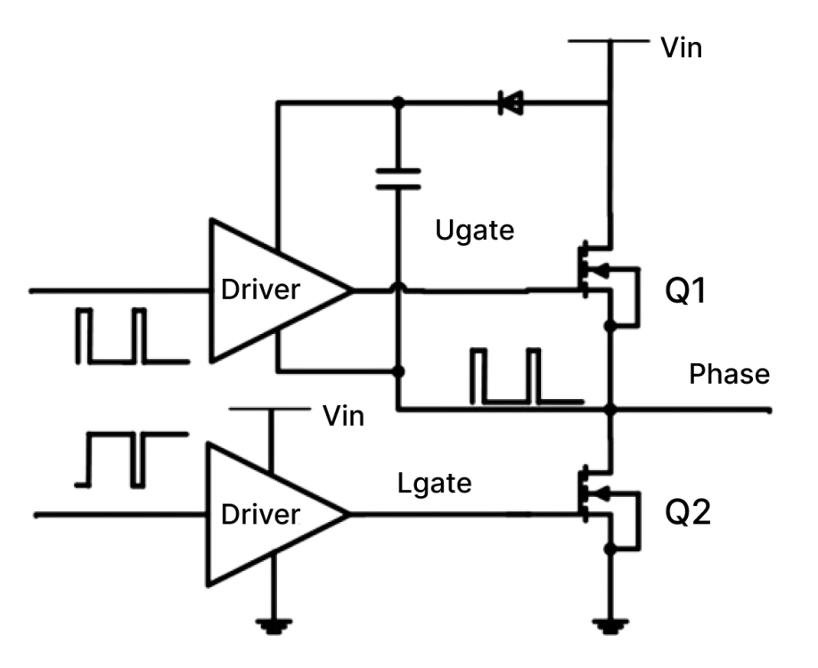
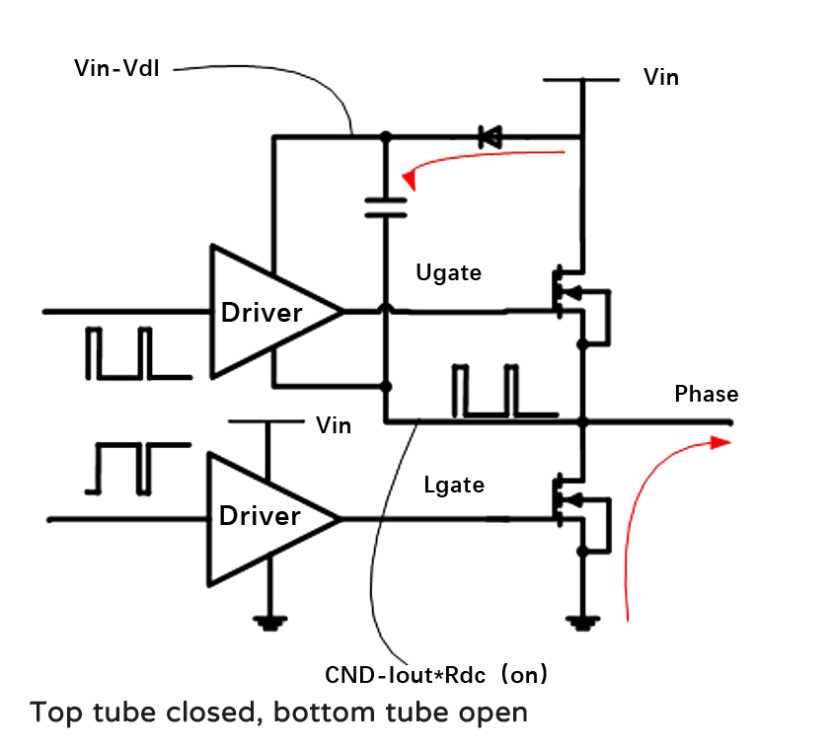
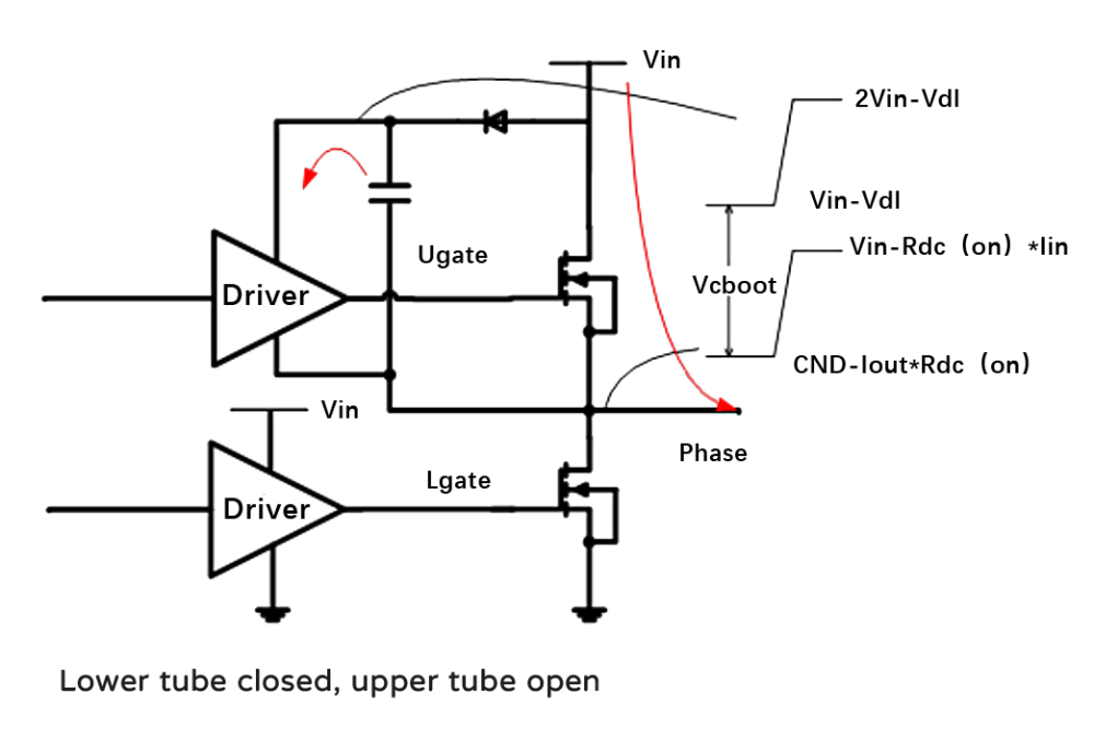
We know that the Buck circuit generally needs a "top tube" to control it, and this realization of raising its own voltage mainly depends on a capacitor, which is the bootstrap capacitor. So how does this capacitor achieve its function? For example, a small capacitor is connected between the GS of the MOS. The MOS charges the capacitor when it is not turned on. When the MOS is turned on, when the S-pole voltage increases, the power supply voltage of the driver above will be automatically increased. At this time, the output voltage of the driver also increases and is connected to the G-pole of the top tube. In other words, the G-pole generates high voltage, and there is enough voltage difference Vgs between the G-pole and the S-pole, so the top tube MOS continues to be turned on. During the charging process, the IC will prohibit the upper and lower tubes from being turned on at the same time to prevent direct conduction. In other words, the upper tube will be turned off and the lower tube will be turned on, and then the diode D1 and the bootstrap capacitor C1 will form a charging circuit. The input power passes through D1, C1, the lower tube, and finally to the ground (negative pole of the power supply), forming a loop to charge the capacitor so that the voltage on both sides of the capacitor is equal to the input power. Conversely, when the lower tube is turned off, the previous loop is naturally cut off, and D1 is in reverse cutoff. At this time, the capacitor will keep the voltage change continuous, and the Vc voltage will gradually decrease with discharge without sudden changes. However, during the charging process, since the capacitor has been charged, the Vc voltage is approximately Vin, so the Vgs of the upper tube is also equal to the input power supply, and this voltage is enough to turn on the upper tube. In this way, a PWM cycle is completed, which is the charging and discharging process of the bootstrap capacitor.
- Earlier
-
 Stardom Jackets changed their profile photo
 -
Note: Operate under the root user by default. 1. Qemu and Debootstrap Installation Since a Debian file system is built on Ubuntu, these two tools can be installed directly using the apt-get command. The commands are as follows: sudo apt-get install binfmt-support qemu qemu-user-static debootstrap 2. Extracting Debian File System Use the debootstrap command to extract the file system. Execute the following command to retrieve the file system from the Debian mirror: mkdir /home/forlinx/debian sudo debootstrap --arch=armhf --foreign buster root https://mirrors.tuna.tsinghua.edu.cn/debian/ Explanation of command parameters: arch:Specify CPU architecture buster:Debian version (currently 10) foreign:Use when initializing unpacking in a different architecture than the host root:The folder where the file system is stored https: // mirrors.tuna.tsinghua.edu.cn / debian /:Download source Extraction may take around 10 minutes. Please be patient. Successful extraction reveals the Linux directory tree. If extraction fails, try multiple attempts or switch networks. 3. Perfecting the File System Since the operation is conducted on an X86 virtual machine, QEMU needs to be used to simulate an ARM environment to improve the file system. a.To copy qemu-arm-static into the newly built base system, use the following command: cd root sudo cp /usr/bin/qemu-arm-static usr/bin cd .. b.Initialize the file system. Execute the following command: sudo DEBIAN_FRONTEND=noninteractive DEBCONF_NONINTERACTIVE_SEEN=true LC_ALL=C LANGUAGE=C LANG=C chroot root debootstrap/debootstrap --second-stage c.Use the chroot root command to initialize file system chroot root d.Use the command to create the following echo "proc /proc proc defaults 0 0" >> etc/fstab mkdir -p usr/share/man/man1/ mknod dev/console c 5 1 e.To update the download sources, use the command vi /etc/apt/sources.list to open the source.list file and replace the contents with the following: deb http://mirrors.ustc.edu.cn/debian stable main contrib non-free #deb-src http://mirrors.ustc.edu.cn/debian stable main contrib non-free deb http://mirrors.ustc.edu.cn/debian stable-updates main contrib non-free #deb-src http://mirrors.ustc.edu.cn/debian stable-updates main contrib non-free #deb http://mirrors.ustc.edu.cn/debian stable-proposed-updates main contrib non-free #deb-src http://mirrors.ustc.edu.cn/debian stable-proposed-updates main contrib non-free Then save and exit. Use the command apt-get update to update the source. If updating the download source reports an error,use the date command to modify the system time to solve the problem. f.Use the command apt-get install vim to install some necessary software apt-get install vim apt-get install sudo apt-get install dpkg apt-get install bzip2 apt-get install net-tools apt-get install ntpdate g.Create a new user with the command adduser forlinx, then enter the password adduser forlinx h.Set the root password, use the command passwd root, and set the password to forlinx. passwd root i.To set up Ethernet, enter the following command: vi /etc/network/interfaces As follows: #/etc/network/interfaces -- configuration file for ifup(8), ifdown(8) #The loopback interface auto lo iface lo inet loopback #Wireless interfaces iface wlan0 inet dhcp wireless_mode managed wireless_essid any wpa-driver wext wpa-conf /etc/wpa_supplicant.conf iface atml0 inet dhcp #Wired or wireless interfaces auto eth0 #iface eth0 inet dhcp #iface eth1 inet dhcp iface eth0 inet static address 192.168.0.232 netmask 255.255.255.0 gateway 192.168.0.1 broadcast 192.168.0.255 auto eth1 iface eth1 inet static address 192.168.1.232 netmask 255.255.255.0 gateway 192.168.1.1 broadcast 192.168.1.255 #Ethernet/RNDIS gadget (g_ether) #... or on host side, usbnet and random hwaddr iface usb0 inet static address 192.168.7.2 netmask 255.255.255.0 network 192.168.7.0 gateway 192.168.7.1 #Bluetooth networking iface bnep0 inet dhcp Add a network reboot cd etc/rc5.d/ vi /etc/rc5.d/S02net_restart.sh As follows: #!/bin/bash echo "network restarting!" /etc/init.d/networking restart echo "network restart complete!" j.Modify host name vi /etc/hostname Modify to: Debian k.Modify the system time zone cp /usr/share/zoneinfo/Hongkong /etc/localtime ntpdate ntp.aliyun.com Take East Zone 8 as an example, other time zone files are also included under this path. l.Since 6ull is weak, skip installing the desktop and go straight to using the exit m.Just exit the qemu environment exit 4. Package the file system Go to the debian filesystem directory and use the command tar - cjf rootfs.tar.bz2. / * to package it. 5. Burn-in verification Place the packaged file system into the burner, while keeping the other images as they are and only replacing the file system. Then proceed with the burn-in test. 6. Debian command a.Check Debian version cat /etc/issue b.Install wget apt-get install wget Solve ERROR: The certificate of ‘packages.microsoft.com’ is not trusted. Report error,then add -- no - check - certificate after the command. Appendix: Installation Method for .net on Linux 1. Download the .net compressed package from the official website https://dotnet.microsoft.com/en-us/download/dotnet/6.0 2. Enter the /home/root directory cd /home/root 3. Install script settings vi install.sh The script is as follows: #!/bin/sh DOTNET_FILE=dotnet-sdk-6.0.402-linux-arm.tar.gz export DOTNET_ROOT=$(pwd)/.dotnet mkdir -p "$DOTNET_ROOT" && tar zxf "$DOTNET_FILE" -C "$DOTNET_ROOT" export PATH=$PATH:$DOTNET_ROOT:$DOTNET_ROOT/tools DOTNET_FILE is the name of the downloaded zip file. 4. Execute the installation chmod u+x install.sh ./install.sh 5. Modify environment variables vi /etc/profile As follows: export DOTNET_ROOT=$HOME/.dotnet export PATH=$PATH:$HOME/.dotnet:$HOME/.dotnet/tools 6. Test Enter the following command: dotnet new console -o sample1 cd sample1 dotnet run The following output should be seen: Hello World!
-
 A water level indicator detects and indicates the level of water in an overhead tank and relays the information back to a control panel to indicate whether the tank has a high or low water level. In this tutorial, I am going to use the ULN2003 IC to create a simple, inexpensive water level indicator. Using this circuit you can easily control the wastage of water and electricity. Watch this video, for detailed step by step instructions on how to build this circuit and to know how this circuit works. Towards the end of the video I will also discuss whether its really worth building this circuit. Components Required For this tutorial we need: 1 x ULN2003 IC 8 x Different Color LEDs 8 x 1K Resistors 1 x 220Ohm Resistor 1 x Buzzer A Long Ribbon Cable, and A Breadboard or a Custom Built PCB About The ULN2003 IC The notch on the top indicates the starting and stopping points of the numberings of the chip. Starting from left to right going counterclockwise this is the Pin number 1 of the IC. On the left hand side Pin 1 to 7 are the Base Inputs. On the right hand side Pin 10 to 16 are the Collector Outputs. Pin 9 is the Common Cathode node for flyback diodes (required for inductive loads). And, Pin 8 is the Common Emitter shared by all channels of the IC. This pin is typically tied to ground. The UNL2003 IC contains 7 High Voltage, High Current NPN Darlington Transistor Arrays each rated at 50V, 500mA in a 16-pin DIP package. You can connect the IC directly to a digital logic (like Arduino or Raspberry Pi, TTL or 5V CMOS device) without an external dropping resistor. The ULN2003 is known for its high current and high voltage capacity. The Darlington pairs can be "paralleled" for higher current Output. To know more about this IC, please check out my "Tutorial No. 51: All About ULN2003 IC", the link is in the description below. Circuit Diagram The circuit is very simple. I have connected 7 LEDs to the 7 OUT Pins of the IC via 1K Resistors. On my left, are the 7 digital inputs which are connected to a ribbon cable. The other end of the ribbon is submerged in the water tank with exposed terminals at various heights to detect the water levels. Along with the 7 wires, there is an eighth wire that stays at the bottom of the tank and is connected to the +ve terminal. As the tank starts filling up, the water level rises and a conductive path is created between the positive terminal and the base of Darlington Transistor inside the IC. Hence a logic HIGH is sent to the Input Pin of the IC which leads to the corresponding OUT Pin to go LOW lighting up the LEDs one by one starting from the bottom Red to the top Green. The bottom Red LED indicates lack of water and the top Green LED indicates that the tank is 100% full. You can also add a buzzer to the circuit to get an audio indication when the tank is full. If you want to be super funky, you can also add a relay module which can turn on and off the water pump. Breadboard Demo Before assembling the components on a PCB, lets do a quick test on a breadboard to make sure our logic works as expected. For this demo, I am going to fill up a coffee mug with normal tap water. As you can see, the LED indicators go up from bottom Red to the top Green as I keep filling the mug. The buzzer starts buzzing when the mug is 100% full. Hence, our setup is working as expected. The Board So, this is how my board looks like in 2D and 3D. If you want to learn how to design a PCB, please check out my "Tutorial No. 45: Transformers PCB BADGE", the link is in the description below. Component Assembly Now, lets solder the components to the board. Lets first solder all the resistances to the board. Then, lets solder all the LEDs to the board. I am using a 3mm Green LED as the power indicator. Next, I am soldering the IC base to the board. Since I care a lot about my ICs and micro-controllers, I never solder them directly to the board. In case of an ICs, I always try to use an IC bases or if a base is not available I use female pin headers. After soldering the IC base, I am soldering the Buzzer to the board. Now to conclude the setup, I am soldering the Ribbon Cable to the board. For my setup, I am only using half a meter long cable. But in a real-world scenario, you will definitely need a cable longer than this. Final Demo So, this is how the final setup looks like. As the water level rises, a conductive path is created between the positive terminal and the base of Darlington Transistors inside the IC. This triggers a logic HIGH at the Input Pins of the IC and the corresponding OUT Pins goes LOW lighting up the LEDs one by one starting from the bottom Red to the top Green. When the mug is 100% full the top green LED lights up and we also hear a noises of the buzzer. Usability To be very frank, I see more disadvantages than advantages of using this IC in building a liquid level indicator. You may have a different opinion, but my opinion is based on the below facts: The choice of the probes that will remain submerged in the liquid has to be done very carefully as they: Rust, foul and deteriorate due to "corrosion" and "electrolysis" causing the LEDs to slowly fade and finally turn off. Hence the probes need to be cleaned and replaced every 2 - 3 years. This circuit will work well with tap water, however do not use this with salt water or with any flammable liquid. If in your house you get hard-water, there will be salt deposits on the probes and you will have to clean the salt deposits on a regular basis. This circuit will not work if you have a metal tank. Replacing the contact points with something "non-corrosive" may help but I will not put my bet on that. Another option is to have "large electrodes" which will have a low impedance even when covered with impurities. To conclude I would like to say that the ULN2003 is not the best device to use for this application. You might be better using a "CMOS buffer" or inverter which needs less water conductivity to operate and also gives a more sudden output change as the input voltage rises and falls, along with "non-corrosive large electrodes". Thanks Thanks again for checking my post. I hope it helps you. If you want to support me subscribe to my YouTube Channel: https://www.youtube.com/user/tarantula3 Video: View Full Blog Post: View References GitHub: View Gerber: View DataSheet: Download All About ULN2003 IC: View Transformers PCB BADGE: View DIY Relay Module: View Support My Work BTC: 1Hrr83W2zu2hmDcmYqZMhgPQ71oLj5b7v5 LTC: LPh69qxUqaHKYuFPJVJsNQjpBHWK7hZ9TZ DOGE: DEU2Wz3TK95119HMNZv2kpU7PkWbGNs9K3 ETH: 0xD64fb51C74E0206cB6702aB922C765c68B97dCD4 BAT: 0x9D9E77cA360b53cD89cc01dC37A5314C0113FFc3 LBC: bZ8ANEJFsd2MNFfpoxBhtFNPboh7PmD7M2 COS: bnb136ns6lfw4zs5hg4n85vdthaad7hq5m4gtkgf23 Memo: 572187879 BNB: 0xD64fb51C74E0206cB6702aB922C765c68B97dCD4 MATIC: 0xD64fb51C74E0206cB6702aB922C765c68B97dCD4 Thanks, ca gain in my next tutorial.
 -
 VBsemi is proud to introduce the new TO220 package VBM115MR03 designed specifically for high-voltage applications. With its excellent performance and reliability, this product has become an ideal alternative to traditional high-voltage products. Excellent performance: Ultra-high withstand voltage: The VBM115MR03 design supports voltages up to 1500V to ensure stable operation in harsh high-voltage environments and ensure the safety and reliability of the system. Very low on-resistance: The low on-resistance of only 6000 milliohms effectively reduces energy consumption and heat dissipation requirements, improves system efficiency, and extends equipment life. Powerful current-carrying capacity: The maximum current reaches 3A, allowing VBM115MR03 to easily handle the high load requirements in most industrial and consumer electronics applications and ensure stable operation. With its excellent performance, VBM115MR03 has become the first choice for engineers designing high-voltage circuits. It is widely used in industrial automation, power conversion, medical equipment, electric vehicle charging systems, and other fields, with extraordinary reliability and capability. Benefits & Highlights: Wide compatibility: VBM115MR03 has excellent compatibility and can directly replace a variety of high-voltage products, including but not limited to IRFBG30, SiHFBG30, IXTP3N120, etc., providing engineers with greater flexibility and choice. Stable and reliable: After strict quality control and comprehensive performance testing, it ensures that the VBM115MR03 maintains stable electrical performance and reliability in long-term use, reducing maintenance costs and risks. Diverse applications: VBM115MR03 are widely used in key fields such as industrial control systems, power converters, medical equipment, and electric vehicle charging systems, providing efficient and reliable solutions for various application scenarios. With these advantages, VBM115MR03 stands out in high-voltage circuit design and is ideal for engineers to choose a reliable solution. Apply: VBM115MR03 is widely used in many key areas, including but not limited to the following: Industrial automation control system: In industrial automation, VBM115MR03 is the core component of motor drive, power management and electrical control system to ensure the reliable operation of equipment in high-voltage environments. Power conversion and inverter: As a key component of power converters and inverters, VBM115MR03 can efficiently convert and manage electrical energy, and are suitable for solar inverters, grid-connected and off-grid energy systems, ensuring stable and efficient energy conversion. Medical devices: In medical devices, VBM115MR03 are used for high-voltage power management, precision control circuits, electrical isolation, etc., to ensure the safe operation and precise control of medical devices, including imaging equipment, surgical instruments, and monitoring equipment. EV Charging Systems: VBM115MR03 EV charging systems provide charging efficiency and circuit safety, support fast charging and long-term use, and meet the stringent requirements of the EV market for efficient energy management and reliability. VBM115MR03.pdf
 -
1. Product Description Vending machines, combining modern technology with the idea of convenient shopping, have become essential in our lives. It breaks through the constraints of time and space, providing us with round-the-clock uninterrupted product purchasing services. Whether in busy transportation hubs or quiet residential areas, you can always find its presence. 2. Components: Body Compartment: Made from high-strength, corrosion-resistant metal materials to ensure the stability and durability of the vending machine. The warehouse's interior is well-designed and can be adjusted according to the size of the goods to maximize the use of storage space. Payment System: Integrated with multiple payment methods including coins, bills, card swiping, and mobile payments, satisfying various consumer payment needs. Display and operation: HD touchscreen shows product information and purchase process, simplifying steps to enhance user experience. Product Delivery System: Uses precise mechanics and sensors for accurate, fast delivery to the outlet after payment. Communication Management System: Enables real-time monitoring, sales data analysis, and remote fault diagnosis and repair of vending machines via wireless network. Business Logic Topology The vending machine's main control system acts as its operational core, akin to its "brain", overseeing and coordinating each module's functions. With the ongoing development of IoT, big data, and AI, automation has become an inevitable trend in the vending machine industry. This has led to new demands for the main control systems, focusing on: Core Controller: It is essential to choose a stable, reliable, and high-performance core controller to ensure the overall logic control and data processing capabilities of vending machines. Device Stability: It requires 24/7 uninterrupted operation, necessitating high stability and durability in both hardware and software. Specifically, the software system should have fault self-check and automatic recovery capabilities. Scalability and Compatibility: To meet various scenarios and demands, the main control system of vending machines needs to be scalable. As products evolve, the main control system should be compatible with new hardware and software standards. Payment Security: As payment methods diversify, ensuring the security of the payment process has become increasingly important. Vending machines need to guard against various security threats, such as data breaches and fraudulent activities. AI Integration: Vending machines need to have intelligent recognition capabilities and data analysis abilities to recommend products based on users' purchasing preferences. FET3568-C system on module(SoM) from Forlinx Embedded Systems offers high performance, low power consumption, and rich functionality, making it ideal for vending machines for these reasons: Powerful Performance: FET3568-C SoM is based on the Rockchip RK3568 processor, which features a quad-core 64-bit Cortex-A55 architecture with a clock speed of up to 2.0GHz. It supports lightweight edge AI computing and delivers strong computational and processing capabilities. Such performance meets the high demands of logic control and data processing for vending machine control systems, ensuring efficient and stable operation of the vending machines. Rich Interfaces and Expandability: The FET3568-C SoM offers 3 x PCIe slots, 4 x USB ports, 3 x SATA3.0 controllers, and 2 x Gigabit Ethernet ports. It supports 5 x display interfaces including HDMI2.0, eDP, LVDS, RGB Parallel, and MIPI-DSI, with up to three simultaneous display outputs. These interfaces provide great convenience for expanding the functionality of vending machines, enabling customized development to meet various scenarios and requirements. Multi-OS Support: FET3568-C SoM supports multiple operating systems including Linux, Android 11, Ubuntu, and Debian 11. This flexibility allows developers to choose the most suitable operating system according to actual needs, thereby simplifying the software development process and improving development efficiency. Meanwhile, Forlinx Embedded has made numerous optimizations in software, such as introducing a 4G watchdog process. This design ensures that the 4G communication function can automatically recover after a disconnection, significantly improving the stability and reliability of the vending machine's network communication. Advanced Security: In terms of security, the FET3568-C hardware can integrate encryption chips and trusted root modules. These hardware-level security measures provide solid protection for system information security. The ability to verify software integrity and authenticity from the hardware level effectively prevents the intrusion of malicious software and the risk of system tampering. High Stability: FET3568-C has undergone rigorous environmental temperature testing, stress testing, and long-term stability operation testing, ensuring stable and reliable performance in various terminals and operational environments. This is crucial for vending machines that require 24/7 uninterrupted operation, as it can significantly reduce failure rates and enhance user experience. In summary, the FET3568-C SoM not only features robust performance and stability, but also offers flexible operating system options, optimized software design, rich interfaces, and powerful expandability. These features make it an ideal choice for vending machine control solutions, capable of meeting the evolving needs of the industry.
-

Implementing Web Server on ESP32
isaacatki replied to CETECH's topic in Electronic Projects Design/Ideas
Setting up a web server on the ESP32 sounds like a great DIY project! I was once diving into a similar adventure with my Raspberry Pi. It was such a rewarding experience to see it serve up web pages from our garden shed, controlling our irrigation system remotely. If you're looking to take your project to the next level, consider exploring offshore hosting solutions like Zynoo—they offer robust options that could enhance your project's reliability and security. -
 Let’s create an offline voice-controlled LED system using the DFRobot Beetle ESP32 C6 and the DFRobot Offline Voice Learning Sensor. This project combines hardware components and programming to create an interactive system that responds to voice commands. Here’s a detailed step-by-step guide: 1️⃣Project Overview We’ll build a voice-controlled LED system that turns on and off NeoPixel lights based on spoken commands. The DFRobot Gravity Offline Voice Recognition Sensor will listen for voice input, and the Beetle ESP32 C6 will process the commands and control the LED. Get PCBs for Your Projects Manufactured You must check out PCBWAY for ordering PCBs online for cheap! You get 10 good-quality PCBs manufactured and shipped to your doorstep for cheap. You will also get a discount on shipping on your first order. Upload your Gerber files onto PCBWAY to get them manufactured with good quality and quick turnaround time. PCBWay now could provide a complete product solution, from design to enclosure production. Check out their online Gerber viewer function. With reward points, you can get free stuff from their gift shop. Also, check out this useful blog on PCBWay Plugin for KiCad from here. Using this plugin, you can directly order PCBs in just one click after completing your design in KiCad. 2️⃣Components Needed DFRobot Beetle ESP32 C6: This compact ESP32 board will serve as our microcontroller. DFRobot Gravity Offline Voice Recognition Sensor: An offline voice recognition module with built-in command words and self-learning capabilities. Breadboard and Jumper Wires: For connecting the components. 3️⃣Wiring Diagram Connect the DFRobot Gravity Sensor to the Beetle ESP32 C6 using jumper wires. 4️⃣ Install the Arduino IDE : If you haven’t already, download and install the Arduino IDE. 5️⃣Add the ESP32 Board to Arduino IDE: Follow these steps to add the ESP32 board to your Arduino IDE: Open the Arduino IDE. Go to File > Preferences. In the “Additional Boards Manager URLs” field, add the following URL: https://dl.espressif.com/dl/package_esp32_index.json Click OK. Go to Tools > Board > Boards Manager. Search for “esp32” and install the “esp32” package. Select the Beetle ESP32 C6 as your board under Tools > Board. 6️⃣Download the DFRobot Voice Recognition Library: Visit the DFRobot Voice Recognition Sensor tutorial for detailed steps. Download the DFRobot Voice Recognition Library from the DFRobot website. 7️⃣Write the Arduino Sketch: Create a new Arduino sketch (File > New). Copy and paste the following sample code into your sketch: #include "DFRobot_DF2301Q.h" DFRobot_DF2301Q_I2C DF2301Q; int led = 15; void setup() { Serial.begin(115200); pinMode(led, OUTPUT); while (!(DF2301Q.begin())) { Serial.println("Communication with device failed, please check connection"); delay(3000); } Serial.println("Begin ok!"); DF2301Q.setVolume(7); DF2301Q.setMuteMode(0); DF2301Q.setWakeTime(15); uint8_t wakeTime = 0; wakeTime = DF2301Q.getWakeTime(); Serial.print("wakeTime = "); Serial.println(wakeTime); DF2301Q.playByCMDID(23); // Common word ID } void loop() { uint8_t CMDID = 0; CMDID = DF2301Q.getCMDID(); Serial.print("CMDID = "); Serial.println(CMDID); if (CMDID == 5) { digitalWrite(led, HIGH); } if (CMDID == 6) { digitalWrite(led, LOW); } } 8️⃣Voice Commands: The DFRobot Gravity Sensor comes with 121 built-in fixed command words. You can also add 17 custom command words. For example: “Turn on the lights” “Change color to blue” “Dim the lights” 9️⃣Upload the Sketch: Connect your Beetle ESP32 C6 to your computer via USB. Select the Arduino IDE's appropriate COM port and board (ESP32 Dev Module). Click the Upload button to upload the sketch to your Beetle ESP32 C6. 🔟Test Your Voice-Controlled LED System: Power up your system. Speak the predefined voice commands to control the led ✅Conclusion With this setup, you’ll have an offline voice-controlled LED system that responds to your spoken commands. Feel free to expand the project by adding more custom commands or integrating other devices!
 -
The TS-M1021 is a diminutive Bluetooth module, measuring merely 8 by 12 millimeters, designed for applications requiring minimal size and low power consumption, without compromising on cost-effectiveness. This module is renowned for its remarkable stability and wide-ranging compatibility. It comes with a default setting that facilitates Bluetooth serial port transparent transmission, allowing users to modify serial port baud rates, device names, and additional parameters using the supplied AT commands. This feature enables adaptable operation and straightforward implementation, making the module an ideal choice for a diverse array of customer development projects. Model No.: TS-M1021 Features Bluetooth Version: BLE 5.1 Frequency Band: 2.402GHz-2.480GHz ISM band TX Power: -20dBm~+10dBm Receive Sensitivity: -97dBm Air Rate: 250Kbps/1Mbps/2Mbps Antenna: Ceramic Antenna Advise Range: 100m Memory: 512KB FLASH+56KB RAM Size: 12*8*1.5mm Pin/GPIO: 12/7 Power Supply: 2.0~3.6V Operating Temperature: -40℃~+85℃ Peripheral Interface: UART/I2C/ADC Serial Transparent Transmission Rate: BLE 20KB/s Applications Smart home Location tracking Intelligent educational equipment Measurement and monitoring system Industrial sensors and controls Medical equipment monitoring and wireless control
-
TS-M1020D is an 8*12mm ultra-small size Bluetooth low power ultra-low cost Bluetooth module, the module is a Bluetooth 5.2 chip, integrated BLE+SPP dual Bluetooth protocol, with excellent stability and compatibility. Module default Bluetooth serial port transparent transmission, the user can change the serial port baud rate, device name and other parameters according to the provided AT instructions, flexible operation and simple use. Suitable for various development projects of customers. Model No.: TS-M1020D Features Bluetooth Version: BLE 4.2+SPP 3.0 Frequency Band: 2.402GHz-2.480GHz ISM band TX Power: -20dBm~+4dBm Receive Sensitivity: -95dBm Air Rate: 250Kbps/1Mbps/2Mbps Antenna: Ceramic Antenna Advise Range: 80m Memory: 256KB FLASH+128KB RAM Size: 12*8*1.5mm Pin/GPIO: 12/7 Power Supply: 3.1~4.35V Operating Temperature: -20℃~+85℃ Peripheral Interface: UART/SPI/I2C/ADC Serial Transparent Transmission Rate: BLE 4KB/s, SPP 16KB/s Applications Smart home Location tracking Intelligent educational equipment Measurement and monitoring system Industrial sensors and controls Medical equipment monitoring and wireless control
-
 Ahmad Nurdin changed their profile photo
 -
 Satyadeo Vyas changed their profile photo
 -
 Evelynn changed their profile photo
 -
 Play with Circuit changed their profile photo
 -
 THENNAVAN changed their profile photo
 -
 fabulax style changed their profile photo
 -
 Carlos Daniel Morales changed their profile photo
 -
Introduction to the U-Boot boot process U-Boot Boot Process Stage 1 Main process Partial Hardware Initialization -> Load Full U-Boot into RAM -> Jump to Stage 2 Entry for Execution. Files Used Mainly in Stage 1 (Non-Open Source Scenario): start.S (Hardware Initialization, watchdog, interrupts, clock configurations) lowlevel_init.S (RAM (DDR) initialization, U-Boot code loading, stack setup, BSS clearing, jump to U-Boot Stage 2 U-Boot Boot Process Stage 2 Stage 2 involves further hardware initialization by U-Boot, configuring command line parameters and environment variables, and transitioning to the kernel. The main documents used are: board.c file: Typically, our own files are located in the board/forlinx/ directory. main.c file: Located in the common directory Main function Some of the more important initialisation functions are as follows: 1.''setup_mon_len'' function: Set the ''gd'' structure's ''mon_len'' member variable, representing the length of the entire code; 2.''initf_malloc'' function: Sets the ''gd '' structure's member variables related to ''malloc''; 3.''board_early_init_f''function; 4.To initialize the IO configuration of the serial port, defined in the board/freescale/mx6ull_toto/mx6ull_toto.cfile; 5.''timer_init'' function: Initialize the kernel timer to provide clock ticks for U-Boot, defined in the ''arch/arm/imxcommon/timer.c''file; 6.''get_clocks'' function: Retrieve the clock for the SD card peripheral (sdhc_clk), defined in the arch/arm/imxcommon/speed.c file; 7.''init_baud_rate'' function: Initialize the baud rate, defined in the ''common/board_f.c'' file. 8.''serial_init'' function: Initialize serial communication settings, defined in the''drivers/serial/serial.c''file; 9.''console_init_f'' function: Initialize the console, defined in the ''common/console.c'' file; 10.''display_options'' function: Print U-Boot version information and compilation details, defined in the lib/display_options.c file; 11.''print_cpuinfo'' function: To display CPU information and the main clock frequency, defined in the arch/arm/imx-common/cpu.c file; 12.''show_board_info'' function: Print development board information, defined in the common/board _ info.c file; 13.''init_func_i2c'' function: To initialize I2C; 14.''announce_dram_init'' function: This function is simple, it outputs the string "DRAM:"; 15.''dram_init'' function: Doesn't actually initialize DDR but rather sets the value of gd->ram_size. Current U-boot startup print information U-Boot SPL 2021.01-gd1345267-dirty (Jul 08 2023 - 08:00:49 +0800) SYSFW ABI: 3.1 (firmware rev 0x0015 '21.5.1--w2022.07-am62x (Terrifi') am625_init: board_init_f done(counter=1) SPL initial stack usage: 13768 bytes i2c_write: error waiting for data ACK (status=0x116) i2c_write: error waiting for data ACK (status=0x116) Auth Success! normal mode am625_init: spl_boot_device: devstat = 0x1843 bootmedia = 0x9 bootindex = 0 Trying to boot from MMC1 am625_init: spl_boot_device: devstat = 0x1843 bootmedia = 0x9 bootindex = 0 Loading Environment from MMC... MMC: block number 0x3500 exceeds max(0x2000) *** Warning - !read failed, using default environment am625_init: spl_boot_device: devstat = 0x1843 bootmedia = 0x9 bootindex = 0 am625_init: spl_boot_device: devstat = 0x1843 bootmedia = 0x9 bootindex = 0 init_env from device 9 not supported! Starting ATF on ARM64 core... NOTICE: BL31: v2.5(release):v0.6-6-gd489c56b NOTICE: BL31: Built : 15:08:18, Jun 26 2023 U-Boot SPL 2021.01-gd1345267-dirty (Jul 08 2023 - 08:00:56 +0800) SYSFW ABI: 3.1 (firmware rev 0x0015 '21.5.1--w2022.07-am62x (Terrifi') am625_init: board_init_f done am625_init: spl_boot_device: devstat = 0x1843 bootmedia = 0x9 bootindex = 0 Trying to boot from MMC1 am625_init: spl_boot_device: devstat = 0x1843 bootmedia = 0x9 bootindex = 0 U-Boot 2021.01-gd1345267-dirty (Jul 08 2023 - 08:00:56 +0800) SoC: AM62X SR1.0 Model: Forlinx OK62xx-C board DRAM: 2 GiB MMC: mmc@fa10000: 0, mmc@fa00000: 1 Loading Environment from MMC... OK In: serial@2800000 Out: serial@2800000 Err: serial@2800000 52334 bytes read in 5 ms (10 MiB/s) Saving Environment to MMC... Writing to MMC(0)... OK Net: eth0: ethernet@8000000 Autoboot in 1 seconds switch to partitions #0, OK mmc0(part 0) is current device SD/MMC found on device 0 Failed to load 'boot.scr' Failed to load 'uEnv.txt' MMC: no card present 20208128 bytes read in 111 ms (173.6 MiB/s) 52334 bytes read in 5 ms (10 MiB/s) 4595 bytes read in 5 ms (897.5 KiB/s) ## Flattened Device Tree blob at 88000000 Booting using the fdt blob at 0x88000000 Loading Device Tree to 000000008fef0000, end 000000008fffffff ... OK U-boot shortens 2 seconds of boot time by disabling USB and Ethernet via defconfig.Modify the autoboot.c file to hardcode bootdelay=0, reducing it by 1 second. diff --git a/common/autoboot.c b/common/autoboot.c index e628baff..685779b6 100644 --- a/common/autoboot.c +++ b/common/autoboot.c @@ -328,10 +328,11 @@ const char *bootdelay_process(void) int bootdelay; bootcount_inc(); - +/* s = env_get("bootdelay"); bootdelay = s ? (int)simple_strtol(s, NULL, 10) : CONFIG_BOOTDELAY; - +*/ +bootdelay = 0; if (IS_ENABLED(CONFIG_OF_CONTROL)) bootdelay = fdtdec_get_config_int(gd->fdt_blob, "bootdelay", bootdelay); Comment out the function that reads uEnv.txt file. Remove useless printed information. Cropped Log 16:33:00:290 U-Boot SPL 2021.01-gd1345267-dirty (Jul 25 2023 - 16:14:18 +0800) 16:33:00:303 SYSFW ABI: 3.1 (firmware rev 0x0015 '21.5.1--w2022.07-am62x (Terrifi') 16:33:00:351 am625_init: board_init_f done(counter=1) 16:33:00:351 SPL initial stack usage: 13768 bytes 16:33:01:527 i2c_write: error waiting for data ACK (status=0x116) 16:33:01:527 i2c_write: error waiting for data ACK (status=0x116) 16:33:01:527 Auth Success! 16:33:01:544 normal mode 16:33:01:544 am625_init: spl_boot_device: devstat = 0x1843 bootmedia = 0x9 bootindex = 0 16:33:01:544 Trying to boot from MMC1 16:33:01:729 Loading Environment from MMC... MMC: block number 0x3500 exceeds max(0x2000) 16:33:01:749 *** Warning - !read failed, using default environment 16:33:01:749 16:33:01:776 am625_init: spl_boot_device: devstat = 0x1843 bootmedia = 0x9 bootindex = 0 16:33:01:795 am625_init: spl_boot_device: devstat = 0x1843 bootmedia = 0x9 bootindex = 0 16:33:01:795 init_env from device 9 not supported! 16:33:01:795 Starting ATF on ARM64 core... 16:33:01:795 16:33:01:812 NOTICE: BL31: v2.5(release):v0.6-6-gd489c56b 16:33:01:812 NOTICE: BL31: Built : 15:08:18, Jun 26 2023 16:33:02:990 16:33:02:997 U-Boot SPL 2021.01-gd1345267-dirty (Jul 25 2023 - 16:14:43 +0800) 16:33:02:997 SYSFW ABI: 3.1 (firmware rev 0x0015 '21.5.1--w2022.07-am62x (Terrifi') 16:33:02:997 am625_init: board_init_f done 16:33:03:022 am625_init: spl_boot_device: devstat = 0x1843 bootmedia = 0x9 bootindex = 0 16:33:03:022 Trying to boot from MMC1 16:33:04:507 16:33:04:507 16:33:04:507 U-Boot 2021.01-gd1345267-dirty (Jul 25 2023 - 16:14:43 +0800) 16:33:04:507 16:33:04:507 SoC: AM62X SR1.0 16:33:04:508 Model: Forlinx OK62xx-C board 16:33:04:530 DRAM: 1 GiB 16:33:04:593 MMC: mmc@fa10000: 0, mmc@fa00000: 1 16:33:04:640 Loading Environment from MMC... OK 16:33:04:640 In: serial@2800000 16:33:04:640 Out: serial@2800000 16:33:04:640 Err: serial@2800000 16:33:04:654 51701 bytes read in 6 ms (8.2 MiB/s) 16:33:04:654 using kernel dtb display control 16:33:04:685 Saving Environment to MMC... Writing to MMC(0)... OK 16:33:04:701 Net: eth0: ethernet@8000000 16:33:04:701 Autoboot in 0 seconds 16:33:04:748 switch to partitions #0, OK 16:33:04:748 mmc0(part 0) is current device 16:33:04:795 SD/MMC found on device 0 16:33:05:104 3229642 bytes read in 141 ms (21.8 MiB/s) 16:33:05:228 20075008 bytes read in 111 ms (172.5 MiB/s) 16:33:05:228 51701 bytes read in 6 ms (8.2 MiB/s) 16:33:05:244 4575 bytes read in 5 ms (893.6 KiB/s) 16:33:05:285 ## Flattened Device Tree blob at 88000000 16:33:05:285 Booting using the fdt blob at 0x88000000 16:33:05:306 Loading Device Tree to 000000008fef0000, end 000000008fffffff ... OK 16:33:05:306 16:33:05:306 Starting kernel ...
-
In some high-frequency switching circuits, the Miller effect of MOS tubes has the unpleasant disadvantages of extending the switching frequency, increasing power consumption, and reducing system stability. As shown in the figure below, there is a small flat step between t2 and t3, and the blue straight line part is the "Miller platform". MOS tube conduction (Miller effect): When MOSFET is turned on, Vds starts to drop and Id starts to rise, at which time MOSFET enters the saturation region; but due to the Miller effect, Vgs will not rise for a period of time, at which time Id has reached the maximum, and Vds continues to drop until the Miller capacitor is fully charged, and Vgs rises to the value of the driving voltage. At this time, MOSFET enters the resistance region, at which time Vds drops completely and the turn-on ends. Miller effect: Since the Miller capacitor prevents the rise of Vgs, it also prevents the fall of Vds, which will prolong the loss time and increase the loss. The left figure below is the circuit symbol diagram of the MOS tube, and the right figure is the equivalent model of the MOS tube. Miller capacitance shown in the figure Cgs: GS parasitic capacitance Cgd: GD parasitic capacitance Input capacitance Ciss = Cgs + Cgd Output capacitance Coss = Cgd + Cds Reverse transfer capacitance Crss = Cgd Miller effect refers to the effect of the equivalent input capacitance value being amplified by the distributed capacitance Cgs between the input and output under the effect of inverting amplification. The Miller effect will form a Miller platform. Disadvantages of Miller effect: From the first figure, we can see that under inductive load, the switching process of the MOS tube is significantly prolonged due to the Miller effect. The longer the D and S poles of the MOS tube overlap, the greater the conduction loss will be. Miller capacitance is bound to exist due to the manufacturing process of MOS tubes, so it cannot be completely eliminated. However, we can reduce the impact of the Miller effect by reducing the gate resistance Rg. It can be seen that the smaller R1 is, the faster gs is charged and the faster the MOS tube is turned on. However, is the Miller effect really useless? We know that everything has two sides, and the existence of the Miller effect is bound to be so. We can use the Miller effect to achieve the purpose of slow start of the circuit. By increasing the gate resistance of the MOS tube and connecting a large capacitor in parallel between the G-D poles of the MOS tube, the Miller step can be artificially lengthened. The circuit in the figure below increases the parallel capacitance between the gate resistance and the G-D pole, increases the Miller step, and turns the output waveform into a triangular pulse.
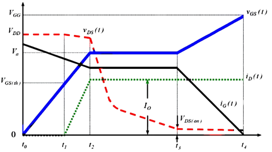
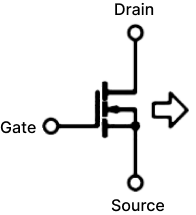
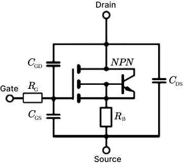
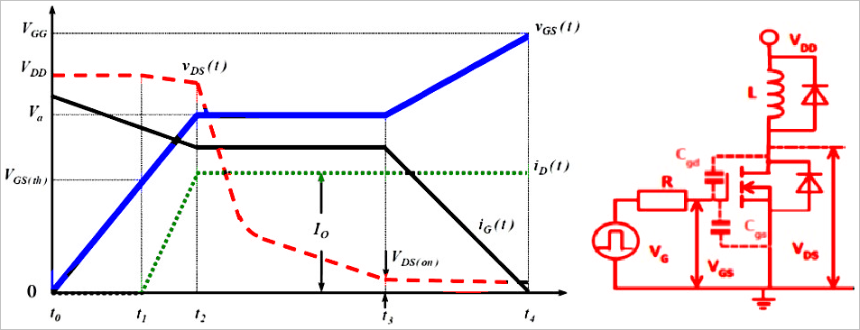
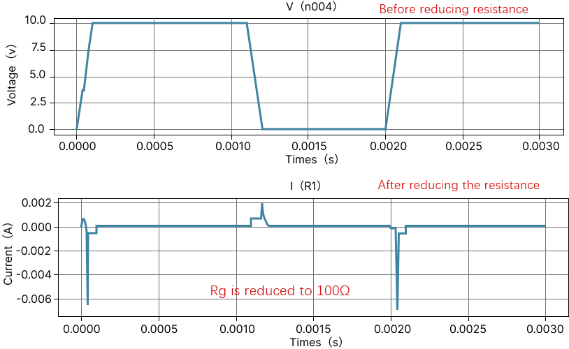
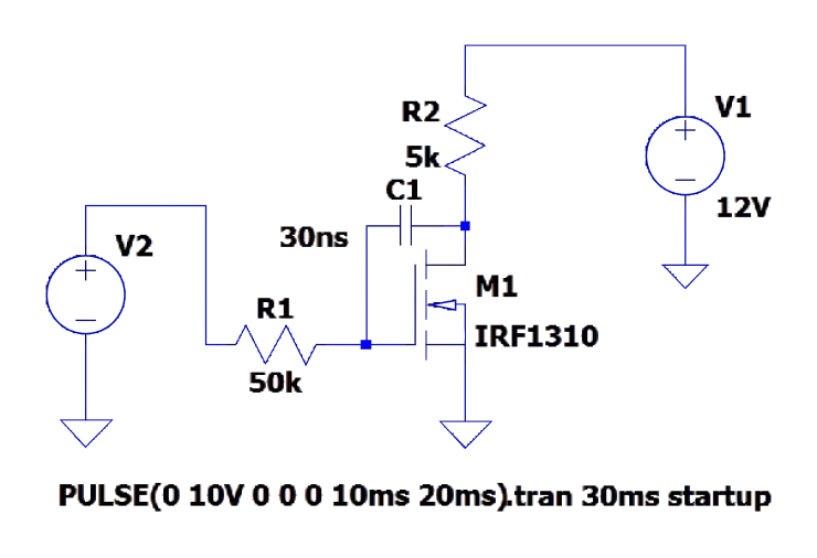

-
 As a popular single-board computer, the Raspberry Pi's powerful functionality and flexible scalability make it an ideal choice for a variety of projects and applications. During development, using a Raspberry Pi-adapted test board can significantly simplify hardware integration and functional verification. The functions and features of the Raspberry Pi test board Hardware expansion and interface compatibility: Raspberry Pi test boards are usually designed to be compatible with different models of Raspberry Pi, providing additional GPIO pins, USB interfaces, camera ports, etc. to support richer hardware expansion and peripheral connections. Functional verification and performance testing: The test board simplifies the verification and performance testing of Raspberry Pi hardware functions. They provide a platform that is closer to the actual deployment environment, helping developers identify and resolve potential hardware issues or compatibility challenges early on. Integrated development environment supports: Test boards adapted to Raspberry Pi are usually equipped with various tools and documents required for development, such as circuit diagrams, sample codes and operation manuals, which help developers start projects and solve problems more quickly. IoT and sensor applications support: For IoT and sensor applications, the test board may integrate specific sensor interfaces or communication modules, such as Wi-Fi, Bluetooth, LoRa, etc., to facilitate the development of smart devices and data collection systems. E15-LW-T1 is a test board specially developed by Ebyte Efor the mini PCI-e interface module. It is mainly aimed at the embedded application of the E106 series LoRa gateway module launched by our company, and is equipped with ESD protection. Supports multiple systems and multiple baud rates. Developers can easily connect a variety of peripheral devices through jumpers according to actual needs.
 -
 This project aims to develop a real-time image processing system using the Xilinx Zynq UltraScale+ MPSoC XCZU19EG-2FFVC1760I. The system leverages the FPGA fabric and ARM Cortex processors available on the MPSoC to perform image processing tasks efficiently. The project demonstrates how to interface image sensors, process image data in real-time, and display processed results using appropriate peripherals. Introduction The field of image processing is crucial in various applications such as robotics, medical imaging, surveillance, and more. Real-time processing of images requires both high computational power and efficient data handling capabilities. The Xilinx Zynq UltraScale+ MPSoC provides a unique advantage with its combination of FPGA for hardware acceleration and ARM processors for general-purpose computing, making it ideal for such applications. Objectives: To design a system capable of capturing images from a camera module. To implement real-time image processing algorithms on the FPGA fabric. To utilize ARM Cortex processors for interfacing, control, and display purposes. To demonstrate the performance advantages of using FPGA acceleration for image processing tasks. Materials and Methods: Hardware Components: Xilinx Zynq UltraScale+ MPSoC XCZU19EG-2FFVC1760I development board. High-resolution image sensor module. HDMI display interface for output visualization. Necessary power supplies and peripherals. Software Tools: Xilinx Vivado for FPGA design and synthesis. Xilinx SDK for ARM Cortex software development. OpenCV or similar libraries for image processing algorithms. Methodology: 1. System Architecture Design: Configure the Zynq MPSoC to interface with the image sensor module. Design FPGA fabric to preprocess images (e.g., filtering, edge detection). Implement ARM Cortex processors for system control and user interface. 2. Image Processing Algorithms: Select appropriate algorithms for real-time image enhancement or feature extraction. Implement these algorithms using HLS (High-Level Synthesis) for FPGA acceleration. Optimize algorithms for both FPGA and ARM execution. 3. Integration and Testing: Integrate FPGA and ARM components into a cohesive system. Test functionality with different input scenarios and evaluate real-time performance. Verify results by displaying processed images on an HDMI monitor. Results: The project aims to achieve real-time image processing capabilities using the Xilinx Zynq UltraScale+ MPSoC. Results will include performance metrics such as processing speed, resource utilization, and quality of processed images. Comparative analysis with CPU-only or GPU-based solutions may also be included to highlight the advantages of FPGA-based acceleration. Conclusion: This project demonstrates the feasibility and advantages of using the Xilinx Zynq UltraScale+ MPSoC for real-time image processing applications. By leveraging FPGA hardware acceleration and ARM processors, the system achieves high-performance image processing capabilities suitable for various embedded applications. Future work may focus on expanding the system’s capabilities or optimizing algorithms further. References: Xilinx Zynq UltraScale+ MPSoC datasheet and technical documentation. Research papers and articles on FPGA-based image processing. Online resources and community forums for FPGA and embedded systems development.
-
1. RTC Description 1.1 What's RTC? RTC (Real Time Clock): It is an electronic device that functions like a clock to output real-world time. RTC Overview: The RTC is a 32-bit timer that increments every second, functioning like a clock. Date and time can be modified by adjusting the timer value. To ensure that the RTC time is not lost during power outages, a small battery is usually connected separately to provide power to the RTC. Once the small battery is removed, the RTC will lose the time after a power outage. However, the time in the lower right corner of the computer and the time seen with date under Linux are not RTC time. During system operation, a high-precision register on the chip serves as the system time reference. To avoid drift over extended system operation and prevent time loss after power failure, each time the system starts up, it retrieves the time from the RTC to set as the system time. 1.2 Difference Between Internal and External RTC External RTC advantages: Low power consumption Minimal deviation Therefore, an external RTC (Real-Time Clock) is generally used. 2. Unix Time Stamp Unix timestamp is defined as the number of seconds elapsed since 00:00:00 coordinated Universal Time (UTC) on January 1, 1970, excluding leap seconds. The timestamp is stored in a seconds counter, which is a 32-bit/64-bit integer variable. The timestamp is stored in a 32-bit/64-bit integer seconds counter, uniform globally across all time zones, with local times derived from applying offsets to this counter. 3. Common operation 3.1 Date The "date" command can read/write the current system time and also display the time zone. Common operations: View time: View timezone Set time: 3.2 Timezone modification The time zone file is/etc/localtime. When the time zone needs to be modified, only the corresponding time zone file needs to be linked to/etc/localtime. 3.3 hwclock Read RTC time Write in time Note: If UTC is enabled and the time zone is modified, hwclock -wu should be usedSync system time to RTC Sync RTC time to system 4. Sync RTC to system At system startup, the RTC time is read and used as the system time. Using the example of the imx6ull processor, after powering on, the operations related to RTC are as follows: There are the followings in the /etc/rcS.d/S55bootmisc.sh: The main functions of this part are: Call the/etc/init.d/hwclock.sh with the parameter start Read the timestamp /etc/timestamp and compare it to the existing system time, if the timestamp is further back, write the time in the timestamp to the system via date, and then call /etc/init.d/hwclock.sh again with the parameter stop; The followings are in the /etc/init.d/hwclock.sh: ...... [ "$UTC" = "yes" ] && tz="--utc" || tz="--localtime" case "$1" in start) ...... if [ "$HWCLOCKACCESS" != no ] then if [ -z "$TZ" ] then hwclock $tz --hctosys else TZ="$TZ" hwclock $tz --hctosys fi fi ...... stop|restart|reload|force-reload) ...... if [ "$HWCLOCKACCESS" != no ] then hwclock $tz --systohc fi if [ "$VERBOSE" != no ] then echo "Hardware Clock updated to `date`." fi exit 0 ;; ...... The main functions of this part are: When UTC is enabled, assign the tz variable to "--utc" and vice versa to "--localtime". When the parameter is start, execute hwclock $tz --hctosys to synchronise hardware time to system time; If $UTC is yes, the time read is considered to be UTC time, and vice versa for localtime. The main difference here lies in whether the system interprets the read time as UTC time, and adjusts the time according to the timezone pointed to by /etc/localtime. For example, in the current time zone (UTC+8), if the --utc option is added, the system will add 8 hours to the read time. If --utc is not added, or --localtime is used, the system will consider the read time as the current time and will not make any adjustments. Note that hwclock -w by default writes the system time. hwclock -w writes the current system time to the RTC (Real-Time Clock); hwclock -wu by default writes UTC time. Taking East 8 as an example, hwclock -wu is to write the current system time minus 8 hours to the RTC; When the parameter is stop, execute hwclock $tz --systohc to write the system time to the hardware RTC. As mentioned earlier, when the timestamp is later, it will enter this branch; "If $UTC is yes, it is considered that the time to be written is UTC time; otherwise, it is considered to be localtime." The main difference here is that if the --utc parameter is added, the system adjusts the system time obtained from date before writing it to the hardware RTC. Conversely, without the parameter, the system writes the time directly to RTC. Taking East 8 as an example, if the --utc parameter is added, the current system time minus 8 hours to the RTC. If --utc is not added, or --localtime is used, the system will write the current system time in hardware RTC; Note: The full name of hctosys is hardware clock to system. The full name of systohc is system to hardware clock. "timestamp" originates from: There are the followings in ls /etc/rc6.d/S25save-rtc.sh: Due to the system's runlevel being 5, during startup it runs scripts from /etc/rc5.d, as evident from the printed messages during boot. Printing information is as follows: ...... echo -e "\033[32mupdate timestamp\033[0m" date -u +%4Y%2m%2d%2H%2M%2S 2>/dev/null > /etc/timestamp ...... When reboot is called, you can see the printed information added: root@fl-imx6ull:~# reboot ...... update timestamp Unmounting remote filesystems... urandom stop: failed. Deactivating swap... Unmounting local filesystems... reboot Restarting system Conclude that the current system time is written to the timestamp when reboot is executed. After the next boot, the system time will definitely be later than after the last reboot. 5. RTC Test Please note: The following examples are based on the GMT+8 time zone. Case 1: Set the RTC time manually to an earlier date, for example, 2022. At this point, executing a reboot will set the current time as a timestamp eight hours ahead, which will then be written to the hardware clock. System time after reboot is: At this point, if you power off the board for about ten minutes to ensure the RTC battery remains charged, and then power it on again, you will see that the board's time is: The timestamp remains the same. Case 2: Set the RTC time manually to an earlier date, for example, 2022. Use ntpdate to synchronize the time, then execute a reboot to trigger the update of the timestamp. The updated timestamp is the system time minus 8 hours. At this point, if you power off the board for about ten minutes to ensure the RTC battery remains charged, and then power it on again after ten minutes, the board's time will be: The timestamp remains the same. Case 3: Use hwclock -w to directly write the system time to the RTC, then power off without updating the timestamp, and power on again. At this point, the timestamp remains unchanged, but the system time has moved back by 8 hours. Case 4: Read the RTC time directly as the system time, then power off directly and power on again. Note that the system time has to be later than the timestamp time in order not to be affected by timestamps. After booting again, the system adds eight hours to the RTC time as the system time, so the time is normal. 6. Common Problems 6.1 Loss of time due to power outage Check whether the software writes the time to the RTC. Measuring small cell voltage Check the number of RTC devices under/dev. Generally, there are two. If there is only one, it means that the external RTC is not recognized. 6.2 External RTC is not identified First, scan the I2C bus with I2C tools to see if the I2C address of the RTC chip can be found. The address for RX8010 is 0x32, and for PCF8563 it's 0x51. If the address cannot be found, troubleshooting hardware involves checking soldering, crystal oscillators, power supply, and replacing the chip if necessary. If the device is found but displays a numeric I2C address, it likely indicates that the corresponding device driver is not correctly loaded. Here are steps for troubleshooting and resolving this issue: If the device is found and displays ''UU,'' this scenario is unlikely to occur. If encountered, troubleshooting can be approached from these aspects: checking system boot logs for print information, examining the RTC loading section, and verifying if there are any kernel errors; investigating hardware for address conflicts. RX8010 root@fl-imx6ull:~# i2cdetect -r -y 0 0 1 2 3 4 5 6 7 8 9 a b c d e f 00: -- -- -- -- -- -- -- -- -- -- -- -- -- 10: -- -- -- -- -- -- -- -- -- -- -- -- -- -- -- -- 20: -- -- -- -- -- -- -- -- -- -- -- -- -- -- -- -- 30: -- -- UU -- -- -- -- -- -- -- -- -- -- -- -- -- 40: -- -- -- -- -- -- -- -- -- -- -- -- -- -- -- -- 50: -- -- -- -- -- -- -- -- -- -- -- -- -- -- -- -- 60: -- -- -- -- -- -- -- -- -- -- -- -- -- -- -- -- 70: -- -- -- -- -- -- -- --
-
Fast Pesticide Residue Detector: Efficient and convenient device for rapid analysis of pesticide residue in fruits and vegetables. It accurately measures pesticide residue in agricultural products, ensuring food safety and dietary health. It is widely used in industrial and commercial administration, vegetable wholesale markets, supermarkets, shopping malls and other fields. Hardware Technology Implementation Features High Sensitivity and Accuracy: The detector employs advanced detection technology, capable of detecting very low concentrations of pesticide residues, ensuring precise and sensitive test results. Fast Detection and High Throughput: Utilizing advanced electronic and optoelectronic systems, the pesticide residue detector provides quick and accurate test results, enhancing detection efficiency. Some models also handle large sample volumes, further enhancing their high-throughput detection advantage. Automation and User-friendliness: It uses automated control technology to perform testing processes such as sample introduction, detection, and cleaning automatically, reducing manual operation time and errors. User-Friendly Interface: Its intuitive design simplifies operation, requiring minimal specialized skills. Versatility and Wide Applicability: In addition to pesticide residue detection, some pesticide residue analyzers also offer multiple detection methods to meet various pesticide testing needs. This makes the instrument valuable across various fields such as agricultural product quality and food safety. With food safety concerns increasingly prominent, pesticide residue detection has become a crucial step in ensuring food quality and safety. Traditional pesticide analyzers are often limited by processing capabilities and power consumption, hindering rapid and accurate detection demands. Forlinx Embedded recommends the FET3568-C SoM as the solution. FET3568-C is a high-performance, low-power processor, particularly suitable for embedded devices and IoT applications. In pesticide residue analyzers, the FET3568-C platform provides robust support for efficient operation with its outstanding computational power and power management capabilities. With powerful computing power. The powerful CPU cores can process large volumes of data to finish the pesticide residue detection and analysis within a short time. This is crucial for scenarios requiring real-time detection and output of results, effectively enhancing detection efficiency. Excellent power consumption control In the pesticide residue analyzer, low power consumption means extended battery life, which is crucial for users who need to conduct long-term detection in fields or laboratories. Additionally, low power consumption helps reduce device heat generation, thereby enhancing device stability and reliability. Rich peripheral interfaces such as UART, SPI, I2C, etc., facilitate communication with various sensors and external devices. In the pesticide residue analyzer, these interfaces can connect key components such as photodetectors and sensors, enabling rapid data acquisition and transmission. Additionally, the RK3568 supports various storage media, making it convenient for users to save and export test data. In addition to hardware performance improvements, the FET3568-C also enables software optimization for pesticide residue analyzers. Based on the powerful computing capabilities of RK3568, the analyzer can run more complex algorithms and models, thereby improving detection accuracy and precision. Additionally, the RK3568 supports various operating systems and programming environments, providing developers with flexible development options. Rockchip's RK3568 significantly enhances the performance and reliability of pesticide residue analyzers. Its powerful computing capabilities, excellent power management, and rich peripheral interfaces enable pesticide residue analyzers to better meet the demands for rapid and accurate detection, providing robust technical support for food safety.
-
 https://arduino.stackexchange.com/questions/51092/6-wire-3-digits-7-segment-display-and-arduino-question
 -
The Raspberry Pi 5 is a powerful platform for various projects, including implementing large language models (LLMs) like OLLAMA. In this article, we’ll guide you through installing and using OLLAMA on your Raspberry Pi 5. What is OLLAMA?🤖 OLLAMA is not an LLM itself but a tool that facilitates the running of various open-source AI models on your device. It handles the downloading and operation of supported language models and provides an API for application interaction. Why Use OLLAMA on Raspberry Pi 5?🥷: Data Privacy: All data processing occurs locally, enhancing security. Offline Capabilities: Operates without an internet connection, ideal for remote areas. Real-time Processing: Local deployment can reduce latency compared to cloud-based services. Get PCBs for Your Projects Manufactured You must check out PCBWAY for ordering PCBs online for cheap! You get 10 good-quality PCBs manufactured and shipped to your doorstep for cheap. You will also get a discount on shipping on your first order. Upload your Gerber files onto PCBWAY to get them manufactured with good quality and quick turnaround time. PCBWay now could provide a complete product solution, from design to enclosure production. Check out their online Gerber viewer function. With reward points, you can get free stuff from their gift shop. Also, check out this useful blog on PCBWay Plugin for KiCad from here. Using this plugin, you can directly order PCBs in just one click after completing your design in KiCad. Equipment Needed⚙️: Raspberry Pi 5 (8GB recommended) Micro SD Card with Raspberry Pi OS installed Stable internet connection for initial setup Basic familiarity with command-line operations 1️⃣ Updating Raspberry Pi OS: Update your Raspberry Pi’s OS to ensure all packages are current. sudo apt update sudo apt upgrade Verify that curl is installed: sudo apt install curl 2️⃣Run the OLLAMA Installer: Next, we need to download and install the Ollama on the Raspberry Pi. Navigate to the Ollama site and download the Linux version. Execute the following command in the terminal to install OLLAMA: curl -fsSL https://ollama.com/install.sh | sh 3️⃣Running OLLAMA: After installation, you can run OLLAMA using the command: ollama run phi --verbose Replace [model_name] with your chosen AI model. For instance, TinyLlama will be less resource-intensive than Llama3. Wait until the installation is done. Once the installation is done, now our LLM will wait for our questions. Just enter the questions and wait for the answer. 4️⃣Optimizing Performance: Memory Management: Run the Raspberry Pi in CLI mode without the desktop loaded to save resources. Performance Tuning: Adjust settings for better performance on limited hardware. Conclusion With OLLAMA, you can leverage the power of LLMs directly on your Raspberry Pi 5. Whether you’re a hobbyist or a developer, this setup allows you to maintain data privacy, work offline, and enjoy real-time processing. Follow the steps outlined above to get started with OLLAMA on your Raspberry Pi 5.
-
Marine instrument panels are critical display and monitoring devices on ships, crucial for ensuring maritime safety, efficiency, and comfort. Real-time monitoring of vital ship information such as position, speed, heading, and engine status through marine instrument panels enables prompt adjustments and decision-making. They not only enhance the precision and reliability of ship operations but also help reduce accident risks, ensuring safe navigation. Moreover, the digital and intelligent design of marine instrument panels allows crew members to manage and control ships more efficiently, improving operational efficiency. They are key tools for ship operation and management. With the continuous advancement of maritime technology, there is an increasing demand for intelligence and digitization in modern ships. As a core component for ship information display and monitoring, the performance and stability of marine instrument panels are crucial to meet modern maritime needs for information display, data monitoring, and navigation safety. Specific objectives include: Providing a clear and intuitive instrument display interface enables crew members to quickly access navigation information. Facilitating compatibility with various data interfaces enables seamless data transmission with onboard sensors and equipment. Ensuring that instrument panels can operate stably in harsh maritime environments, with high resistance to interference and waterproof performance, is essential. Based on the above characteristics, the hardware platform of modern marine instrument panels should possess the following features: High-performance processor: Ensures fast response and accurate display of navigation information, equipped with powerful data processing and graphic rendering capabilities. Rich Data Interfaces: Integrated with multiple data interfaces such as display ports, serial ports, Ethernet ports, USB ports, etc., enabling seamless connection with various sensors and devices onboard ships for easy data display, real-time acquisition, and transmission. Reliability Design: The hardware itself demands high quality and stability to ensure long-term reliable operation in harsh maritime environments. Based on a modern marine instrument screen hardware platform, Forlinx Embedded recommends FET3588J-C as the hardware development solution. Product Characteristics High-performance processor: Quad-core 64-bit Cortex-A72 + quad-core Cortex-A55 architecture with integrated 6 TOPS NPU for enhanced AI learning and edge computing capabilities in diverse operational scenarios. Rich Display Interfaces: Offers multiple interfaces such as HDMI, eDP, DP, MIPI-DSI, supporting various display types including up to 8K output, meeting diverse requirements for maritime instrumentation screens. At the same time, it supports four-screen display function, which enables the crew to monitor multiple important parameters at the same time and improve work efficiency. High-efficiency Graphics Processing: Integrates ARM Mali-G610 MP4 quad-core GPU, fully compatible with OpenGLES 1.1, 2.0, and 3.2, OpenCL up to 2.2, and Vulkan 1.2. Enables maritime instrumentation screens to efficiently handle complex graphic tasks such as real-time rendering and 3D map display, enhancing user operational experience. Versatile Peripheral Interfaces: Features include dual Gigabit Ethernet, USB 3.1, PCIe 3.0, and 10 UART ports, enhancing data speed and efficiency. This strengthens maritime instrumentation screen functionality, meets navigation needs, and ensures stable data transmission and efficient device communication. Robust and Reliable Performance: The RK3588J platform meets industrial-grade temperature range standards and has undergone rigorous testing to provide stable performance support for high-end applications. During maritime navigation, stable and reliable instrumentation screens are crucial for ensuring the safety of vessels. FET3588J-C SoM's excellent performance ensures reliable operation of the instrumentation screen in harsh environments, providing accurate data feedback to the crew.
-
▊ IP Settings Two IP configuration methods: (1)Set a default static IP; (2)Set a temporary static IP ( it is disabled after power cycling). 1. Static IP settings (1) Open /etc/network/interfaces and modify the configuration vi /etc/network/interfaces As follows, configure eth0 as static and eth1 as dynamic: (2) DNS settings Open rc.local with the command vi /etc/rc.local and add the following to it: echo "nameserver 8.8.8.8" > /etc/resolv.conf (3) Block information update&restart sync reboot 2. Temporary network settings Alternatively, the commands can be used temporarily to set the IP and gateway. However, please note that this method's configuration will be lost after a restart. ▊ Adding Startup Auto-run Content 1. Adding the following to the startup script Enter vi /etc/rc.local As an example of booting with the output ''hello world,'' add the following content: Note: Add the startup auto-run content before exit 0; 2. Adding startup auto-run items To create a startup auto-run item in the /etc/rc5.d/ directory vi /etc/rc5.d/S99test.sh As follows: #!/bin/bash echo "helloworld!" chmod 777 /etc/rc5.d/S99test.sh S99 indicates the startup priority as 99, which can be adjusted by the user based on demand. 3. Power-on self-starting 4G dialing method Previously it was mentioned that startup applications can be directly added to /etc/rc.local. However, 4G slightly differs from other applications because it uses a separate 4G module that requires initialization time. Based on practical tests, the 4G module takes 3-5 seconds after startup to function properly. Therefore, before initiating 4G dialing, a delay of 3-5 seconds is necessary. Modify as follows: vi /etc/rc.local Add the following: Note: The delay time cannot be less than 3s. ▊ WiFi 1. Static IP Settings (WiFi) WiFi login script: /usr/bin/fltest_cmd_wifi.sh The second-to-last line of the script assigns a dynamic IP to wlan0. If there is a need to set a static IP, it can be done as follows: 2. Power-on self-starting settings (WiFi) Also put the WiFi script in the/etc/rc.local. In this case, it is necessary to add an ''&'' symbol at the end to run the script in the background. Otherwise, it might block and prevent access to the file system. ▊ Boot 1. SSH connection failure (1) When SSH cannot connect, check if ping is possible. If ping fails, it could be due to network issues. The computer and the device should be on the same subnet. The default IP for eth0 is 192.168.0.232. Users can directly connect them or connect both to the same router. Then, set a 192.168.0 subnet IP on the computer; (2) If ping is successful, first confirm whether the factory image can connect normally. If the factory image can connect normally, check what services are starting up at boot causing the issue; ensure that services starting at boot are backgrounded. Failure to do so may cause process blocking, preventing SSH login. Consider reflashing the factory image if necessary; (3) Ensure that the board's IP address is being pinged. This can be tested by unplugging the Ethernet cable and then pinging from the computer.
-
 Sophia Camila reacted to a post in a topic:
Fridge Protection
Sophia Camila reacted to a post in a topic:
Fridge Protection
-
Hi Redge, You can build a delay timer circuit to protect your fridge. Here’s a basic outline: 1. **Power Relay**: Use a relay rated for 240V AC and at least 10A (to handle the fridge's startup current). 2. **Delay Timer**: Use an off-delay timer module, adjustable up to 10 minutes. 3. **Wiring**: - **AC IN to Timer**: Connect the AC input to the timer's power input. - **Timer to Relay**: Connect the timer's output to the relay's control input. - **Relay to Fridge**: Connect the relay's switch terminals between the AC input and the fridge. **Operation**: - When AC IN is turned off, the timer starts the delay. - The relay will only activate and supply power to the fridge after the 10-minute delay, even if AC IN is switched back on immediately. Ensure all components are rated for 240V and handle the required power safely. If unsure, consult an electrician for assistance.