

Dave Laurenson
-
Posts
4 -
Joined
-
Last visited
Content Type
Profiles
Forums
Events
Posts posted by Dave Laurenson
-
-
1 hour ago, audioguru said:
I wrongly typed 114A instead of 114W. A single 2N3055 will be at its maximum allowed chip temperature of 200 degrees C when it dissipates 115W and its case is cooled to no more than 25 degrees C with liquid nitrogen or something. A heatsink also gets hot even when it is huge and has a fan blowing on it.
I never operate a transistor anywhere near its maximum temperature, voltage or current. Then it is reliable.
Yes, I did realise the mis-type, and agreed that it wasn't right to operate so close to the maximum. Do you have any comments regarding the use of the 150W rated transistor instead? After all, we are talking about a margin of around 30%...
-
6 hours ago, audioguru said:
Your idea to use only one 2N3055 output transistor will have it burning hot (38V x 3A= 114A!) if the current is set to 3A and the output is shorted or has a very low voltage. Two output transistors share the heat. Their emitter resistors match them pretty well. Two output transistors at b1.5A each will have a higher hFE than only one transistor at 3A then the driver transistor does not need to supply a higher current and it also stays cooler.
Agreed - the 2N3055 is rated at 115W maximum, and as the voltage drop also depends on what the ammeter internal resistance will be, it shouldn't be running so close to its limit. The hFE parameter of the 2N3055 is very loosely defined (as is the case with most BJTs), so one of the transistors could be carrying in excess of 2A, and will run quite a bit hotter than the other, but not a big problem.
Of course, the alternative is to use a single transistor rated with a higher wattage! I wondered about the 2N3771, but couldn't find a spice model for that. I did find a spice model for the FJL4315, which is rated at 230V, 15A and 150W, and has an hFE of 60, so pretty much a drop-in replacement for the 2N3055, and would handle everything the supply could throw at it.
-
On 20/10/2015 at 6:46 PM, liquibyte said:
Many, many questions keep getting asked about this thing and people keep attempting to build it without even knowing the basics, why I don't know. The power supply suffers from a couple of issues that have never really been adequately addressed so this is going to be my attempt at bringing this thing into the modern age. What follows is just preliminary work to right several wrongs I've noticed with the design. It's not complete but I'm posting it to get opinions and suggestions.
This paragraph is for the newbies: DO NOT ATTEMPT TO BUILD THIS YET. If you don't know what you're doing, do not even try and breadboard this. Once I have a final design, I promise that I'll post it.
Now, onward. I'm posting my spice simulation for anyone that wants to try and give this a go. One of the things that concerns me is the power dissipation in the op amps but I'm not sure how to get this down to a more acceptable level because I don't think 150mW at load is very good so suggestions are most welcome.
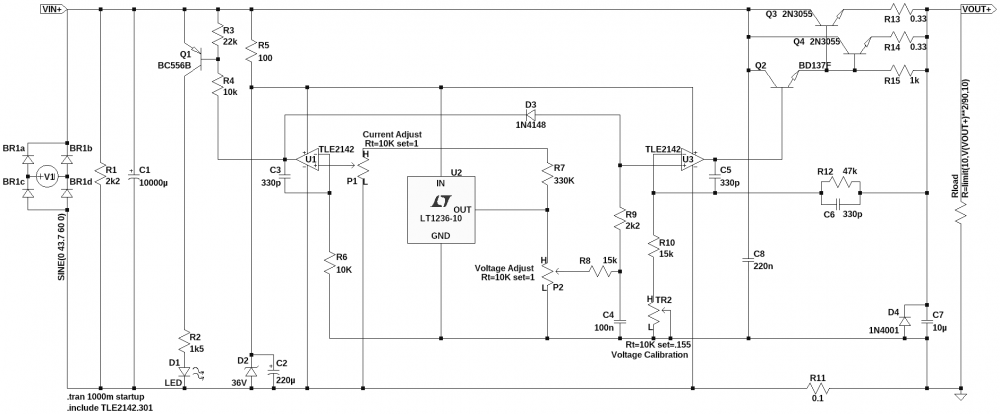
First, the voltage reference in the old version was an extremely odd thing to me so what I wanted to do was get a precision reference in there to work with. 10V seemed like a nice round number so that's what I went with and I actually have one on hand to use.
Second, the sense resistor. 0.47 ohms? Once again, odd. Plus, it suffers from extreme power dissipation as well. My idea is to have a nice 0.1 ohm 3W 4 wire resistor in there to hook a meter to so I adjusted things around the reference to get me to where I wanted to be and I also have some of these.
What I'd like to eventually do is design the meters along with the supply so that what we end up with is a relatively complete project with all the nice bits people seem to be after. No one, I repeat, no one ever offers a suggestion as to what to build to replace this, not one single engineer. They will, however, be the first people to tell you how bad the design is but never offer any sort of advice as to why. I know, I've asked and so have many other people.
Hi All,
I saw this post by Liquibyte, and decided to take up the challenge of offering suggestions. First, I'd like to say that I've enjoyed looking through this thread, and am very impressed with the work that has been done here by Liquibyte, Audioguru and others. I have made some alterations to this new design, BUT I've not yet constructed it. However, there are a number of things that I discovered when simulating with LTspice.
In the attached, I've made a number of alterations - rather than using a diode to ensure that the voltage reference is pulled down only when U1 is active, I've used a transistor. The reason is that if the output were short circuited, then the inverting input of U3 would be zero, so U3 can never get the inverting and non-inverting outputs equal. Hence the current is only limited by the output transistor drive capabilities since the minimum of the non-inverting input is the diode voltage drop plus the minimum output of U1. Instead, I've used a transistor which can pull the non-inverting input of U3 very close to 0V (VIN-), which will be less than VOUT-, so the output of U3 will drop, and cut the voltage at VOUT+.
The second major difference is to remove the unnecessary output transistor Q4. A single 2N3055 can drive up to 15A, so doubling up is not necessary. (In fact, unless the transistors are well matched, it may have no effect whatsoever as at these "low" currents one transistor would carry the bulk of current if the matching were not perfect). I was puzzled by the need for R13 until I realised that this is supposed to be part of circuitry to limit the current output of Q3. I'm assuming that at some point in the past, the diodes that make this work were dropped - perhaps to keep the voltage up under high drive conditions? In the redesign I've added three diodes from VOUT+ to the base of Q2. If U3 tries to drive too much current through Q3, then the excess drive current will be routed through the diode chain, effectively limiting the drive current into Q3. If the voltage is dipping under heavy load currents (less than the limit of 3A), then the output resistor can be reduced in size. However, the consequence is that the maximum output current spike will be higher.
One other final structural modification is to separate the voltage sense and current sense parts of the circuit to allow the common Voltage/Ammeter module to be installed. As I've not built the circuit yet, I don't know what the internal resistance of the ammeter is, so I've put a nominal 0.15Ohm resistor in there. Obviously this should be changed to whatever is appropriate.
With a little reorganisation in the drawing, which includes some test circuits: a 555 astable which has power spikes as it is not decoupled, a resistor that is suddenly shorted out at 0.5s, and a resistor that varies between an almost infinite resistance to zero in a way that should make the current rise linearly up to 0.5s, and then the voltage drop linearly. Also, I've included a period after 1s when the supply is switched off. When I did this, I found it necessary to modify the power supply to U1 to ensure that it continued to limit current, otherwise I ended up with a large current spike after the power source had been removed. I've also added a few notes discussing things I've discovered when changing things around. I'm offering this revised (but note UNTESTED) design to the forum.
Just one note, I've seen pictures of some builds, and am slightly concerned that the casing of 2N3055 is not covered by everyone. The case of the 2N3055 is the collector, which will be at around 38V. If someone connects VOUT- to earth, then the full 38V will be present on the case, with whatever current the transformer can supply. Under the right (i.e. wrong!) conditions, this could be fatal. Please make sure the case is covered!
If anyone builds this, then I'd be really interested to hear how they get on. If you do, please try to understand how the design works first - working with high currents with an untested circuit is not something that should be taken on by those not very familiar with circuit design/construction. My plan is to build a lower current/voltage version of the supply (I really don't need 30V, nor 3A), but finding the time to do this is my biggest problem...
Dave.
0-30V Stabilized Power Supply
in Projects Q/A
Posted
Whether you use one, or multiple transistors, the total power of 114W must be cooled somehow. Unless separate heatsinks are used for each transistor, then the problem still exists. Remember, though, that it is 114W if the outputs are shorted together - that's pretty unusual, so the normal running mode should be a lot cooler anyway.