Search the Community
Showing results for tags 'forlinx'.
-
The default display orientation for the Android interface on the Forlinx Embedded i.MX8MP platform is landscape, but some products may require a portrait display. To address this requirement, Forlinx Embedded provides the following methods for modification: The Android system controls the screen orientation through the persist.vendor.orientation property, which can have values of 0, 90, 180, or 270. Configuration path: frameworks/native/services/su**ceflinger/Su**ceFlinger.cpp Modify in processDisplayHotplugEventsLocked: Su**ceFlinger::processDisplayHotplugEventsLocked() { continue; } + /* Rotate desktop */ + char rotationvalue[PROPERTY_VALUE_MAX] = "";; + property_get("persist.vendor.orientation", rotationvalue, "-1"); + int rotation = atoi(rotationvalue); + ALOGI("Primary Display Orientation is set to rotation %2d.", rotation); + switch (rotation) { + case 0: + internalDisplayOrientation = ui::ROTATION_0; + break; + case 90: + internalDisplayOrientation = ui::ROTATION_90; + break; + case 180: + internalDisplayOrientation = ui::ROTATION_180; + break; + case 270: + internalDisplayOrientation = ui::ROTATION_270; + break; + default: + break; + } + const DisplayId displayId = info->id; const auto it = mPhysicalDisplayTokens.find(displayId); After modification, you need to add the relevant configuration in the environment variable. Path: device/nxp/imx8m/evk_8mp/system.prop persist.sys.timezone=Asia/Shanghai persist.sys.language=zh persist.sys.country=CN +persist.vendor.orientation=90 Rotate 90 degrees here to write 90, 180 degrees to write 180, 270 degrees to write 270. If you encounter a failure to set the value of a property: Add the followings in device/nxp/imx8m/sepolicy/property_contexts; +persist.vendor.orientation u:object_r:debug_prop:s0 vendor.wc_transport. u:object_r:vendor_wc_prop:s0 persist.vendor.usb.config u:object_r:vendor_usb_config_prop:s0 vendor.usb.config u:object_r:vendor_usb_config_prop:s0
-
- android
- vertical screen display
-
(and 3 more)
Tagged with:
-
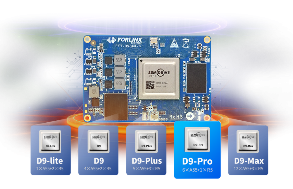
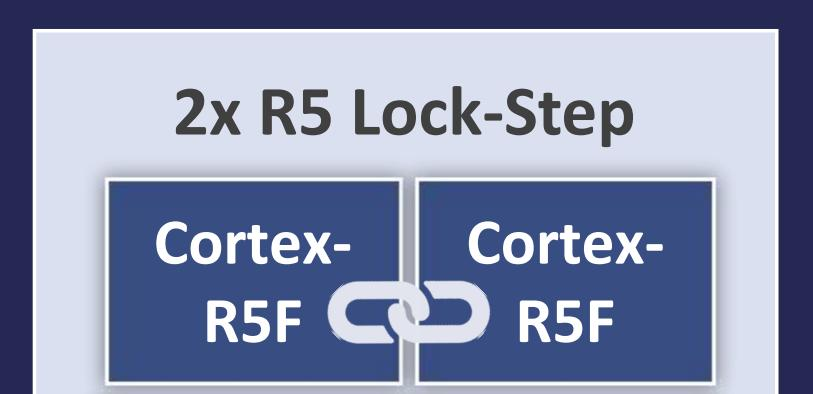
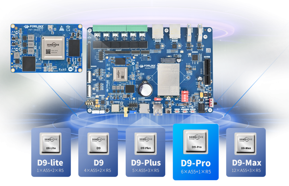
Forlinx Embedded and SemiDrive have teamed up to launch the FET-D9360-C System on Module(SoM), a high-performance industrial processor based on the D9-Pro processor. This SoM is designed to meet the growing demand for high-performance, reliable, and stable computing in the industrial sector. With six ARM Cortex-A55 high-performance cores and one ARM Cortex-R5 real-time core, it offers exceptional computing power and real-time processing capabilities. The D9360 SoM is compatible with multiple processors of the D9 series and is suitable for advanced industrial applications such as industrial IoT devices, industrial robots, and more. Originally published at www.forlinx.net.
-
- forlinx
- fet-d9360-c som
-
(and 2 more)
Tagged with:
-
On November 7th, 2023, Forlinx Embedded launched the Debian 11 system for the first time on their development board, OK3568-C/OK3568J-C, which is based on the RK3568 chipset. Forlinx Embedded officially supports the Debian 11 system on the OK3568-C/OK3568J-C platform. In the field of embedded development, stability and richness are crucial factors. The RK3568, as Forlinx's flagship embedded product, has high performance, low power consumption, and rich interface functions, making it appreciated by industry users. Debian 11 is a stable, reliable, and open-source operating system, which provides a powerful foundation for the OK3568-C. Debian 11 has undergone rigorous testing and validation to ensure system stability, so there is no need to worry about unexpected crashes or data loss. Moreover, Debian 11 has a vast software library, which enables developers to easily install and update required software packages. By combining the advantages of the OK3568-C hardware with Debian 11, developers can fully leverage the diversity of the 3568 hardware interfaces while enjoying the stability and open-source nature of Debian 11. Indeed, this strong combination provides an ideal environment for various embedded projects. When it comes to stability, free and open source, versatility, and vast software libraries, no operating system can rival Debian. Debian is a truly free operating system, and its strength is not only reflected in technology, but also in its active community. Stable Value: Debian stands out for its world-renowned stability. Whether you are building critical business systems or looking for reliable daily desktops, Debian is always the best choice. Debian 11 has undergone rigorous testing and validation to ensure system stability, so there is no need to worry about unexpected crashes or data loss. Free and Open Source: Debian adheres to the concept of free and open source, allowing you to freely use, modify, and share it. This is a truly free operating system. Not only can Debian be obtained for free, but you can also freely view, edit, and distribute its source code. Huge Software Library: Debian has a vast and diverse software library that covers almost any application and tool you can imagine. From office software to entertainment applications, server services to programming tools, Debian has everything in its software library. Not only that, it also provides an easy-to-use package management system, allowing you to easily install and update software. Multi-architecture Support: Debian supports multiple hardware architectures, including x86, ARM, PowerPC, MIPS, etc., making it suitable for various devices and systems. Whether you use a desktop, laptop, server, or embedded device, Debian can provide the ideal solution. Active Community Support: The Debian community is a vibrant place where you can find help, advice, and resources. Both novice and experienced users can participate in the community and receive support. Originally published at www.forlinx.net.
-
As technology develops rapidly, smart devices play an increasingly important role in our lives. Have you ever wondered why your smartphone, computer, and other smart devices can run various complex software and applications? This is all thanks to the powerful processor architecture. Today, we will take you into an eagerly anticipated processor architecture - RISC-V. RISC-V originated from the University of California, Berkeley, and was created by a group of researchers including Andrew Waterman, Krste Asanović, and Yunsup Lee. Their vision is to break the closed design pattern of computer processors and provide an open and flexible instruction set architecture. Since its release RISC-V has received widespread attention in various fields and has become a highly praised architecture. Advantages of RISC-V: 1. Openness and freedom: RISC-V’s open-source allows anyone to use and customize it for free, without paying patent royalties. 2. Modularity and customization: RISC-V’s design allows developers to choose different modules and create custom instruction sets that meet specific needs. 3. Technological innovation: RISC-V’s openness encourages technological innovation and attracts the participation of many companies and research institutions. 4. Wide range of application fields: RISC-V can be used for embedded systems, IoT devices, servers, high-performance computing and other fields. RISC-V is an eagerly anticipated open-source instruction set architecture, with a wide range of application prospects. It represents the future direction of computer processor design, and its openness, freedom, and technological innovation make it have potential in multiple fields. To boost the development of RISC-V, Forlinx Embedded launched a new product - FET7110-C System on Module, which is the first product based on RISC-V architecture. FET7110-C SoM is based on StarFive’s 64-bit high-performance quad-core RISC-V JH7110 processor design and development, with high performance, multi-function, low power consumption characteristics, CPU stable working frequency 1.5GHz, Coremark score of 5.09 CoreMark/MHz, performance better than Cortex-A55. 7110 uses IMG BXE-4-32 MC1 architecture, provides powerful GPU processing capability, supports multi-channel video encoding and decoding, and supports rich functional interfaces such as 2 PCIe2.0, 2 Gigabit Ethernet, and 2 CAN2.0, making its application scenarios more extensive. In terms of power consumption, the FET7110-C SoM is divided into eight power domains that can be switched independently. By using software, the CPU frequency can be adjusted, allowing customers to dynamically control the power consumption according to different application scenarios. FET7110-C SoM is a versatile board for all industries and can be used in many industries such as industrial intelligence, smart surveillance, commercial electronics, smart home and power and energy. After rigorous testing, the FET7110-C SoM can provide stable performance support for customers' high-end applications. The emergence of RISC-V provides a new option. In the future, with the increasing demand for openness and customization, RISC-V is expected to continue to grow in different application fields. In particular, RISC-V is expected to gain more market share in embedded systems, IoT, education and research. Originally published at www.forlinx.net.
-
Saving existing data and avoiding data loss when dealing with sudden power loss is crucial for users of fast storage and acquisition data products. There are many solutions to this problem, among which ferroelectric memory (FRAM) is a good choice. FRAM is a non-volatile memory with fast write speed, capable of storing data in a non-volatile manner while also allowing operations similar to RAM. This article will utilize the Forlinx OK3568-C development board to introduce a solution that employs FRAM - using the SPI0 interface to connect the PB85RS2MC (FRAM) chip. The driver files and application files described in this article can be obtained by contacting Forlinx Embedded's technical support. Modification— To add an SPI device, the following steps need to be taken: Add a description to the device tree → corresponding device driver in the device tree description → device driver added to the kernel Result— Modify OK3568-linux-source/kernel/arch/arm64/boot/dts/rockchip/OK3568-C-common.dtsi Modify the following: Next, we will introduce the adaption process. 1 Driver We searched the menuconfig for fm25, pb85, and other commonly used FRAM words but found that there is no similar driver. So we need to handwrite or port a driver. After searching through various websites, I found a driver for W25Q64. After comparing the various operation codes of PB85RS2MC with W25Q64, I noticed that they are quite similar. Therefore, I have decided to port the W25Q64 driver to PB85RS2MC. According to the description in the PB85RS2MC chip manual, the various opcodes are: Command Name Command Description opcode WREN Write Enable Latch Commands 0000 0110B WRDI Reset Enable Latch CommandWrite Enable Latch Commands 0000 0100B READ Read Command 0000 0011B WRITE Write Command 0000 0010B RDID Read Device Serial Number Command 1001 1111B FSTRD High-speed read command 0000 1011B SLEEP Sleep command 1011 1001B RDSR Read Status Register 0000 0101B WRSR Write Status Register 0000 0001B Therefore, the following opcodes are macro-defined in the driver to be used in the following drivers: First, the initi and exit functions should be carried out in the driver, that is, the spidev _ init and spidev _ exit. The init function is to initialize the character device, register it, etc. The exit function is to release all the things we have registered when we exit. This must match the value of the compatible attribute in the device tree, otherwise the match will be unsuccessful. Furthermore, the driver and the device tree are matched by the value of the compatible attribute, which must be the same as the value of the compatible attribute in the device tree. Otherwise the match will be unsuccessful. The compatible value in the driver is shown below. After the successful matching of the driver and the device tree, we have to execute the probe function, where the probe function performs some initialization and registration of the primary and secondary device numbers. We can determine whether the driver, and the device tree match successfully by whether it prints spi_probe success! Check the read conditions in the PB85RS2MC chip manual, then read the data from the FRAM memory cell, which requires the READ opcode, any 24-bit address entered into the SI. The first spi_transfer structure is used to send the command cmd to the SPI device to prepare the device before reading the data, the second is to send the address to the SPI device, and the third is to receive the data read from the device. This code implements a synchronized read from the SPI device and copies the data to user space. Check the write conditions from the PB85RS2MC chip manual, the WREN command is used to set the write enable latch. The WREN command is required to set the write enable latch before the write operation (WRITE command), and the WRITE command writes data to the FRAM memory cell array. The WRITE opcode, any 24-bit address, and 8-bit write data are input to the SI. The following code implements the function of sending a write enable command to the SPI device. This code implements synchronized writing of data to SPI devices. It sends the write enable command first and then sends the address information and data. The following code writes data synchronously to the SPI device by copying user-space data to the device's transmit buffer and calling the spidev_sync_write function to write the data to the SPI device. 2 Applications To write data to an SPI device, call lseek to change the location of the written data so that data can be written throughout the SPI device, e.g. . /writeframAPP /dev/pb85rs 0 forlinx (0 is the address to write to, forlinx is what to write) To read data from an SPI device, call lseek to change the location of the read data so that it can be read throughout the SPI device, e.g. . /readframAPP /dev/pb85rs 0 (0 is the address of the data to be read) 3 Actual Test (1) First copy fram.ko, readframAPP, writefram APP to any folder in OK3568-C development board. (2) Load the fram.ko module with insmod, spi_probe success! shows that the driver matches the device tree successfully. (3) Look under /dev/ to see if there is a pb85rs device. (4) Use . /writeframAPP /dev/pb85rs 1500 forlinx Write data to the device, 1500 is the address and forlinx is what to write. (5) Use . /readframAPP /dev/pb85rs 1500 (1500 is the address of the data to be read) 4 Power Failure Test Re-reading the PB85RS2MC after a day of power loss revealed that the data was still there. The power-off data retention characteristics of the PB85RS2MC ferroelectric memory chip are verified. At this point, we have completed adding a new SPI ferroelectric memory chip to the OK3568-C development board! Originally published at www.forlinx.net.
-
- spi fram chip
- forlinx
- (and 4 more)
-
In this article, we will introduce the SoMs of the Rockchip. Rockchip x Forlinx Since 2020, Forlinx Embedded has launched three SoM products based on Rockchip RK3399, RK3568, and RK3588 processors and got affirmation and recognition from thousands of enterprise users. 01 RK3588 Series The FET3588J-C SoM is developed and designed based on the Rockchip new generation flagship RK3588J processor, which adopts an advanced 8nm process and integrates quad-core Cortex-A76 + quad-core Cortex-A55, with A76 cores frequency up to 1.6GHz and A55 cores frequency up to 1.3GHz, providing powerful performance support. It supports an 8K ultra-high-definition display and a four-screen heterodyne display, and it is equipped with a wealth of high-speed data communication interfaces to meet the diverse needs of users. After rigorous test, it can operate stably for a long time under -40~+85℃. 02 RK3568 Series FET3568J-C SoM is developed and designed based on Rockchip RK3568J processor, which integrates quad-core 64-bit Cortex-A55 architecture, with frequency up to 1.8GHz and built-in NPU. It is a high-performance, low-power, feature-rich application processor built by Rockchip for the AIoT and industrial markets. The FET3568J-C SoM has been subjected to industrial-grade standard ambient temperature tests, pressure tests, and long-term stability operation tests to ensure its stable and reliable operation. 03 RK3399 Series FET3399-C SoM is the first product jointly launched by Forlinx Embedded and Rockchip. It is based on Rockchip's RK3399 processor design and has two ARM Cortex-A72 cores at 1.8GHz and four ARM Cortex-A53 cores at 1.4GHz; the GPU adopts Mali-T864 and supports OpenGL ES1.1/2.0/3.0/3.1, OpenVG1.1, OpenCL, DX11; 2GB LPDDR3 RAM on board (4GB optional), 16GB eMMC ROM. With its powerful performance configuration, this SoM has been widely used in cutting-edge technology fields such as intelligent self-service terminals, edge computing, 5G intelligent terminals, visual recognition, etc.
-
- rockchip som
- forlinx
-
(and 3 more)
Tagged with:
-
It's honored for Forlinx for the witness and interaction with NXP for the the announcement of i.MX91 SoC a new promising applications processor. As NXP's Gold Partner, Forlinx has kept close touch and communication with NXP since the initial programming of the i.MX91 SoC. As NXP's newest highlight SoC, it's introduced that the i.MX91 SoC delivers an optimized blend of the security, scalability, features, and performance required to enable the next generation of long-life, cost-optimized, and flexible Linux controller platforms for IoT and Industrial applications. ‘i.MX 91 Family X Ecosystem = IoT’ quoted by Robert Thompson the Director of Secure Connected Edge Ecosystem at NXP Semiconductors. We do believe that the premiere of i.MX91 SoC will broaden more users with advanced, cost-optimized and high-security solutions. Here we are pleased to introduce and take you all have a forward-looking at the features of the upcoming i.MX91 based SoM FET-MX91xx-C.

