Capacitor Protection Boards- How do they work?

(*steve*)

¡sǝpodᴉʇuɐ ǝɥʇ ɹɐǝɥd
Moderator
Jan 21, 2010
25,510
Joined
Jan 21, 2010
Messages
25,510
It's probably shunting excess charge through that large transistor.

My guess is that the circuit acts like a glorified zener diode.

The are circuits which use inductors to pump excess charge to an adjacent capacitor, but these are somewhat more complex and I see no inductor.
 

AprilSteel

Feb 2, 2017
111
Joined
Feb 2, 2017
Messages
111
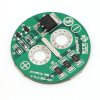
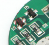
Here is a single board for 1 cap . Perhaps someone can explain how it works from that . There is no LED on this one.s-l1600.jpg
 

AprilSteel

Feb 2, 2017
111
Joined
Feb 2, 2017
Messages
111
It's probably shunting excess charge through that large transistor.My guess is that the circuit acts like a glorified zener diode.

I'm thinking the big one is a diode package rather than a transistor but then thats what a tranny is anyway isn't it. Its marked Q2 on the board
Q2 is marked D1804 on the single one above .Seems to be a tranny at Q1 and something else at U1?

So once it reaches the 2.5Volts it starts leaking current to ground through this zener arrangement?
 
Last edited:

(*steve*)

¡sǝpodᴉʇuɐ ǝɥʇ ɹɐǝɥd
Moderator
Jan 21, 2010
25,510
Joined
Jan 21, 2010
Messages
25,510
I'm thinking the big one is a diode package rather than a transistor

Doubtful, it has 3 connections.

but then thats what a tranny is anyway isn't it.

No, a "tranny" is a transistor. A "diody" is a diode.

Its marked Q2 on the board

Yep, that means it's a transistor

Q2 is marked D1804 on the single one above .Seems to be a tranny at Q1 and something else at U1?

Q1 and Q2 are transistors, U1 is something more complex, I'd bet it's a TL431 or similar.

So once it reaches the 2.5Volts it starts leaking current to ground through this zener arrangement?

That's my guess.

Resistors R4, R5, and R6 are probably there to dissipate some of the energy rather than relying on Q2 to do it all.

This circuit probably doesn't do anything to prevent reverse charging of the capacitors as they discharge. That's another baaad thing.
 

(*steve*)

¡sǝpodᴉʇuɐ ǝɥʇ ɹɐǝɥd
Moderator
Jan 21, 2010
25,510
Joined
Jan 21, 2010
Messages
25,510
Designations aside, the circuit seems very similar to the one I discussed here.

The obvious differences are:
  1. Yours uses a BJT as the pass element
  2. Yours has load resistors to both limit current and to help dissipate heat.
  3. Mine has a pulldown resistor for the gate of the mosfet that is not required in yours due to (1)
  4. The values of the voltage divider resistors are different due to a different "breakdown" voltage.
 

AprilSteel

Feb 2, 2017
111
Joined
Feb 2, 2017
Messages
111
No, a "tranny" is a transistor. A "diody" is a diode.

Diode packages I have seen have an inlet and two identical outlets , diodes going the same way and look like that .

Transistors are tested and have a diode reading base to emmitter and base to collector is what I referred to and they look like that.

So my pick was a diode pack as the diodes both go the same way.
 

(*steve*)

¡sǝpodᴉʇuɐ ǝɥʇ ɹɐǝɥd
Moderator
Jan 21, 2010
25,510
Joined
Jan 21, 2010
Messages
25,510
With a bit of experience you'll realize that a double diode is going to be a very unlikely find in a circuit like this.
 

davenn

Moderator
Sep 5, 2009
14,477
Joined
Sep 5, 2009
Messages
14,477
So my pick was a diode pack as the diodes both go the same way.

With a bit of experience you'll realize that a double diode is going to be a very unlikely find in a circuit like this.

and with a little more experience you would know that D1804 is short for 2SD1804
and a little more experience would tell you that 2SAxxxx and 2SBxxxx transistors are PNP
and 2SCxxxx and 2SDxxxx are NPN type transistors :)

Bob has given a link to the datasheet
 

(*steve*)

¡sǝpodᴉʇuɐ ǝɥʇ ɹɐǝɥd
Moderator
Jan 21, 2010
25,510
Joined
Jan 21, 2010
Messages
25,510
and with a little more experience

Heh, that too.

edit: and V3 on Q1 is likely to be an NPN transistor, and do I see "431" on U1?
 
Last edited:

AprilSteel

Feb 2, 2017
111
Joined
Feb 2, 2017
Messages
111
All interesting thank you kind sirs . Anyone care to perhaps try to draw a circuit for me please?
 

(*steve*)

¡sǝpodᴉʇuɐ ǝɥʇ ɹɐǝɥd
Moderator
Jan 21, 2010
25,510
Joined
Jan 21, 2010
Messages
25,510
All interesting thank you kind sirs . Anyone care to perhaps try to draw a circuit for me please?

Did you check out the link I provided? That should give you the general idea. There is at least one track on the other side of that board that we can't see, so we have to guess where it connects to..

Read the datasheets of the components we've identified (Q1 is unknown, but afaik all sot23 transistors share the same pinout. See if you can confirm its like my circuit.
 

AprilSteel

Feb 2, 2017
111
Joined
Feb 2, 2017
Messages
111
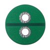
s-l1600Back.jpg
This is the back but I am not having any luck getting a circuit from your circuit . I don't understand what you mean ? Is yours the same circuit . ? I can see some similarities and some major differences.
 

(*steve*)

¡sǝpodᴉʇuɐ ǝɥʇ ɹɐǝɥd
Moderator
Jan 21, 2010
25,510
Joined
Jan 21, 2010
Messages
25,510
That tells me that Q1's emitter is connected to +ve.

Show me the circuit diagram you've managed to draw. I'll check it for you.
 

(*steve*)

¡sǝpodᴉʇuɐ ǝɥʇ ɹɐǝɥd
Moderator
Jan 21, 2010
25,510
Joined
Jan 21, 2010
Messages
25,510
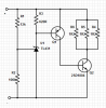
NOTE: R2 is 180k, NOT 100k as shown below.

The first thing to do is to replace the drawings of the components with their schematic symbols, ensuring you connect the wires to the right places:

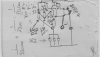
cap-1.png

Note that in drawing this, I made the assumption that the connection between U1 and Q1 is different than shown on your drawing. Check to see if the conductors go as shown below:

s-l1600b.png

Also, the trace between R1 and R2 seems to go under R3.

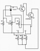
The next step is to rearrange things nicely. positive rail on the top, negative on the bottom, and some sort of left to right order that makes sense.

cap-2.png

And now you have a circuit diagram that you can look at and learn how it operates.
 
Last edited:

AprilSteel

Feb 2, 2017
111
Joined
Feb 2, 2017
Messages
111
Thank You . Testing with a continuity checker confirms the connections you detailed above . My diagram was wrong .I'll now work on understanding what it does. I did have one other question about this circuit . If I were to put an LED in to indicate when the zener was conducting where might it be best put?

Atm I just have it with a diode across the terminals of the ultracap which just flattens the cap
but gives a very pretty light for a while

I have included a pic of another board that lights as each cap reaches about 2.5V so I'm trying to compare and work out where they have the LED across. It appears to be a transistor but I am wondering if I can use one of the small boards transistors in the circuit above or put the LED in series with R4 maybe

The first board I posted does not seem to have an LED on each like this one

Thanks again (*steve*)
 

Attachments

  • IMG_20170301_071043.jpg
    IMG_20170301_071043.jpg
    115.3 KB · Views: 225
  • IMG_20170301_073318_BURST001_COVER.jpg
    IMG_20170301_073318_BURST001_COVER.jpg
    152.1 KB · Views: 211
  • IMG_20170301_073330_BURST001_COVER.jpg
    IMG_20170301_073330_BURST001_COVER.jpg
    168.4 KB · Views: 204
Last edited:

(*steve*)

¡sǝpodᴉʇuɐ ǝɥʇ ɹɐǝɥd
Moderator
Jan 21, 2010
25,510
Joined
Jan 21, 2010
Messages
25,510
You'll have to get me much better photos of those boards if you want me yr try to reverse engineer them.

And why don't you give it a try? Your first effort was pretty good and helped me finish it off.

If that is a LED and a diode directly across the capacitor then it's really not a good way to do it.
 
Top