Need a little help understanding the way my class AB power amplifier works.

Status
Not open for further replies.

tuna

May 25, 2023
4
Joined
May 25, 2023
Messages
4
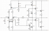
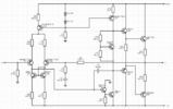
I have an assignment to simulate the given class AB power amplifier. However, it would be nice to get a grasp of what's going on in the circuit (atleast conceptually, no need for 50 equations with 50 variables). I understand the simplest diode biased AB power amp, but this is really too big a step for me. I know the circuit should be divided into smaller parts and see how they interact, but still it's too complicated for me. Any help would be most welcome.
 

Attachments

  • sklop1.png
    sklop1.png
    104.1 KB · Views: 21

crutschow

May 7, 2021
984
Joined
May 7, 2021
Messages
984
It's difficult to discuss the circuit without transistor part designations (Q1, Q2, etc.).
Could you add those to the schematic and repost it?
 

tuna

May 25, 2023
4
Joined
May 25, 2023
Messages
4
Sure, my bad. Tn is npn and Tp is pnp.
 

Attachments

  • sklop1.png
    sklop1.png
    108.1 KB · Views: 96

crutschow

May 7, 2021
984
Joined
May 7, 2021
Messages
984
Okay.
Tp1 and Tp2 form a differential input stage to allow AC and DC negative feedback to stabilize the output.
Tn1 and Tn2 are a current mirror load to provide a high-impedance load for that stage to give a high differential voltage gain.

Tn3 provides a DC drop (similar to that often done by diodes) to bias the output transistor slightly on for AB operation.

R8 provides DC feedback to bias the output to the input ground through the input differential stage so there is no DC bias on the output speaker load.
This is fed back from Tn1 to Tn4 for this purpose.

R9 and C1 attenuate the negative AC feedback through R8 to the differential input, to set the AC circuit gain (to about 10) and reduce the output distortion.

Anything else you want to know?
 
Last edited:

tuna

May 25, 2023
4
Joined
May 25, 2023
Messages
4
Thank you so much, kind stranger. I would just like to know when did you start being able to analyze these circuits so fast. How much hours in the field do I need to be as well versed in electronics as you?
 

crutschow

May 7, 2021
984
Joined
May 7, 2021
Messages
984
I would just like to know when did you start being able to analyze these circuits so fast. How much hours in the field do I need to be as well versed in electronics as you?
That's a difficult question as it depends greatly on your ability to develop an understanding of basic analog electronics.
I have a BS in Electrical Engineering and retired from doing circuit design work in the industry after over 40 years, so I'm not a good judge to remember when I reached the point to readily analyze a new circuit.
Certainly you need to be able to recognize basic circuit functions, such as a transistor amplifier stage (using BJTs and/or MOSFETs), a differential circuit stage, a bias stage, a push-pull output stage, a current-mirror stage, etc., which comes with learning and practice.

Basically you look at each small block in the circuit and try to determine what it is doing in the complete circuit.
Sometimes it's apparent and other times it is not.
 

danadak

Feb 19, 2021
1,064
Joined
Feb 19, 2021
Messages
1,064
Read constantly, read about what you dont know, read diverse areas within the
field..... Build / proto circuits, you are building up your AI memory and skills.


Regards, Dana.
 

AnalogKid

Jun 10, 2015
3,046
Joined
Jun 10, 2015
Messages
3,046
R10, R11, and Tn3 perform as a zener diode. This replaces the diode-bias technique you are familiar with. The temperature tracking is not as good as four diodes in series mounted on the power transistor heatsink, but you can adjust the resistor values so the voltage drop across the transistor more closely matchs the total voltage drop through the four output stage base-emitter junctions. This is a way to reduce the amount of static current through the output transistors needed to eliminate crossover distortion (the "A" part of Class AB).

ak
 

bertus

Moderator
Nov 8, 2019
3,837
Joined
Nov 8, 2019
Messages
3,837

tuna

May 25, 2023
4
Joined
May 25, 2023
Messages
4
Thanks to everyone for the clarification. I discovered a great book on the topic from Bob Cordell: Designing Audio Power Amplifiers. Really learning a tonne here.
Regards, tuna
 

Delta Prime

Jul 29, 2020
2,987
Joined
Jul 29, 2020
Messages
2,987
By breaking the circuit into smaller sections and understanding how these components interact, you can appreciate how a class AB power amplifier efficiently amplifies audio signals
I am addressing the human being behind the artificial intelligence (AI) facade.
Like most things electronics it's about minimizing disadvantages and maximizing advantages it is why when using NPN, PNP transistors in a "push-pull" configuration ,AB amplifiers you get their individual A & B amplifier advantages without their disadvantages but still cannot fully
reproduce audio signals & their efficiency is good for approximately 58% to 78%.
if you can appreciate that!
Then you're lowering your standards
 
Last edited by a moderator:

Delta Prime

Jul 29, 2020
2,987
Joined
Jul 29, 2020
Messages
2,987
A class AB power amplifier is a hybrid electronic amplifier that combines the virtues of class A and class B amplifiers. While class A amps offer linearity but are inefficient, and class B amps are more efficient but prone to crossover distortion, class AB amplifiers mitigate these issues by biasing the output transistors slightly on even at zero input signal. This configuration divides the circuit into three main stages: input, driver, and output.

The output stage employs complementary NPN and PNP transistors, and its biasing uses a diode circuit to eliminate crossover distortion. This amplifier's operation involves signal amplification through these stages, ensuring both halves of the input signal are amplified without distortion, resulting in improved efficiency and fidelity. Simulations using tools like SPICE can illustrate its performance under various conditions.
Gotcha! I was setting you up brother.Hook line and sinker!
But it's all cool; you were just trying to help.Catch and release...
 

WHONOES

May 20, 2017
1,242
Joined
May 20, 2017
Messages
1,242
Additions to the circuit description already supplied.

R2 and R3 connected to the emitters of the Tp1 and Tp2 forming the current mirror will provide a small amount of negative feedback. This will help to linearize the amplifiers response thus reducing distortion. R4 and R5 perform a similar function.

C1 reduces gain to unity at dc. This is important as without it, the small difference between the base emitter voltage on the input transistors will be amplified at the output causing what could be a substantial voltage offset. You would normally expect the output offset voltage, referred to 0V, to be less than 50mV.

Resistor R7 seems to be a bit small in value. 4K7 is more reasonable. At 1K, a sizeable current will be passing through the 1N4148 diodes. There would also normally be a capacitor of 10uF or so in parallel with the 1N4148's to bypass any ripple that may be present on the power supply.

Tn5 forms the voltage amplifying stage and provides most of the circuit gain.

The addition of Tn4 reduces the current load on the input stage thus helping to minimise the output offset voltage,

I have known the circuit comprising R10, R11 and Tn3 as a Vbe multipler for 50 years or so, cos that's what it does.

Tn7 and Tp6 need to be mounted on a heatsink, making sure that they are electrically insulated from each other. Tn3 must be attached to the same heatsink in close proximity.

C2 is called a “Miller Capacitor”. Its function is to make the circuit stable. I tend to connect the end of C2 that is connected to the base of Tp5 onto the output instead, This then includes the output stage in its compensation loop which can make a worthwhile improvement in THD.

Also, your circuit notation for the transistors should be in the format Tr1 Tr2 etc. You do not need to represent the devices polarity within their numbering.
 
Status
Not open for further replies.
Top