DIY Geiger Counter – Looking for Feedback on the Schematic and PCB Design

SmektHet

Aug 12, 2026
1
Joined
Aug 12, 2026
Messages
1
1786544299540.png
1786544321305.png
Hi everyone,

I'm working on a high-voltage circuit and I'd like to get some advice before I order the PCB.

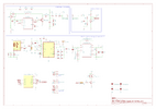
The circuit generates around 400 V at low current. The HV section uses a TLC555-based oscillator, an inductor and a switching transistor to step the voltage up from 5 V to around 400 V. There's also a separate impulse detection section.

The lower part of the schematic is the USB-C/battery charging and 5 V power supply.

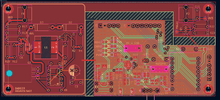
I've attached both my current schematic and PCB layout.

The stack-up is as follows:

  • Signals
  • Ground <- only for LV section
  • Signals / Power
  • Ground <- only for LV section
I'm mainly looking for some advice on the PCB layout:
  1. 1. What's the best way to handle the ground in the HV section? Should I use a copper pour or individual traces?
  2. 2. How much clearance should I leave between the 400 V traces and GND copper?
  3. 3. Are there any particular components or nodes in the schematic that I should give extra spacing around?
  4. 4. Is there anything obviously wrong with having the HV section and the USB/battery circuitry on the same PCB?
  5. 5. Would an isolation slot or something similar be recommended anywhere?

I'd also appreciate any feedback on the schematic itself.

Thanks!
 

Jason Hogan

Aug 5, 2026
1
Joined
Aug 5, 2026
Messages
1
A few practical pointers from building 400V GM tube boards:

  1. HV Ground & Copper Pours: Do NOT pour ground planes directly underneath the 400V boost inductor, rectifier diode, and GM tube anode node. Keep the HV area completely clear of inner and outer ground pours to avoid parasitic capacitive loading on the boost oscillator. Return the HV ground to the main power ground at a single star point near the 5V input cap.
  2. Clearance / Creepage: For 400V DC, aim for at least 2.5mm to 3mm clearance from HV traces to any LV/GND copper (IPC-2221 specifies ~2.5mm for coated boards, but dust/humidity in handhelds eats margin fast).
  3. Critical High-Impedance Nodes: The anode resistor (usually 4.7M to 10M) and the pulse-coupling capacitor node have nanoamp-level currents. Any PCB surface leakage will drag your 400V rail down. Keep those traces as short as possible and wash off all flux residue with IPA after assembly.
  4. Isolation Slots: Milling a 1–1.5mm slot right between the 400V anode pad/diode and the low-voltage detection transistor base/gate is very good practice. It eliminates surface tracking completely.
  5. HV and USB on same PCB: Perfectly fine if physically segregated to opposite ends of the board. Just make sure the fast flyback switching loop (transistor + inductor + diode + catch cap) is as tight as possible so it doesn't couple switching noise into the USB/battery charger lines.
 
Top