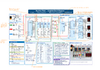
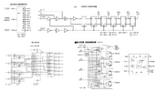
Design and construct a reaction timer

Status
Not open for further replies.

_loma

Oct 13, 2026
1
Joined
Oct 13, 2026
Messages
1
The device should operate as follows:
  1. 1) On reset, all four lights are off and the timer display reads 000.
  2. 2) Start a sequence that turns on one light at a time, with approximately three seconds between lights.
  3. 3) After the fourth light turns on, switch all four lights off simultaneously and immediately start the reaction timer.
  4. 4) Measure elapsed time in milliseconds and show it on three 7-segment displays, from 000 to 999.
  5. 5) Include a Stop button that freezes the timer and holds the measured value on the displays.
  6. 6) Include a Restart button that resets the display and starts the full light sequence again.

    wanna circuit design of this. Can any one help to design it?
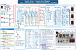
 

Attachments

  • Unknown.png
    Unknown.png
    1.8 MB · Views: 13

Alec_t

Jul 7, 2015
3,821
Joined
Jul 7, 2015
Messages
3,821
Welcome to Electronics Lab.
If this is a school/college/workplace assignment you are expected to post your best effort at doing it, so that we can give guidance where necessary. This is not a homework-done-for-you forum.
 

AnalogKid

Jun 10, 2015
3,056
Joined
Jun 10, 2015
Messages
3,056
wanna circuit design of this. Can any one help to design it?
That schematic is barely OK as a block diagram of the concept, but it has several HUGE errors. Please post a link to the source.

Note that switch debouncing will introduce a short delay / error into the signal timing.

BTW, a 1 ms clock is a frequency of 1.000 kHz. The schematic is riddled with errors such as this, including pinouts, signal connections, pin identifiers, etc.

ak
 
Last edited:

bertus

Moderator
Nov 8, 2019
3,875
Joined
Nov 8, 2019
Messages
3,875
Hello,

I made some comments on the posted schematic:

reaction_comments.png
I have also collected the pin assignments for the used chips:

reaction_chips.png

I have also attached the full datasheets of the used chips.
Read them carefully and try to make a new schematic.

Bertus
 

Attachments

  • ne555_TI.pdf
    569.8 KB · Views: 0
  • cd4017.pdf
    876.1 KB · Views: 0
  • 74HC190.PDF
    108.2 KB · Views: 0
  • 74HC4060.PDF
    569.7 KB · Views: 0
  • 74HC4511.PDF
    88.6 KB · Views: 0

bertus

Moderator
Nov 8, 2019
3,875
Joined
Nov 8, 2019
Messages
3,875
Hello,

Some additional comments:
The 4017 has no clock signal, as noted.
The 555 circuits are incorrect.
The 4060 has no clock signal
You can not have a 3 digit display with 2 counters.
There is no start / stop , reset circuit.

Bertus
 

bertus

Moderator
Nov 8, 2019
3,875
Joined
Nov 8, 2019
Messages
3,875
Hello,

The TS did not return after posting his "schematic" .
He did not even login anymore.
@_loma , please react.

Bertus
 

josephii3

Dec 6, 2024
2
Joined
Dec 6, 2024
Messages
2
The device should operate as follows:
  1. 1) On reset, all four lights are off and the timer display reads 000.
  2. 2) Start a sequence that turns on one light at a time, with approximately three seconds between lights.
  3. 3) After the fourth light turns on, switch all four lights off simultaneously and immediately start the reaction timer.
  4. 4) Measure elapsed time in milliseconds and show it on three 7-segment displays, from 000 to 999.
  5. 5) Include a Stop button that freezes the timer and holds the measured value on the displays.
  6. 6) Include a Restart button that resets the display and starts the full light sequence again.

    wanna circuit design of this. Can any one help to design it?
Before you start drawing the schematic, figure out if you're doing this with discrete logic chips or a microcontroller. If it's a school project for discrete logic, grab a handful of 555 timers and 4026 chips. If you're allowed to use a microcontroller (like an Arduino), this is a 20-minute coding project using a state machine and millis(). The discrete route is way more wiring and debugging.
 
Status
Not open for further replies.
Top