MTS51 schematic for speaker

evol_w10lv

Feb 19, 2013
73
Joined
Feb 19, 2013
Messages
73
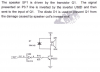
I'm doing a little project on MTS51 Microcomputer trainer using speaker.
Microcontroller: P89C51RC+
Can someone check my schematic?

qwspnh9umkaftns40k4d.png


And what about values C1, C2, C3, R2? I have to search information in P89C51RC+ datasheet or values should be calculated?
 
Last edited by a moderator:

(*steve*)

¡sǝpodᴉʇuɐ ǝɥʇ ɹɐǝɥd
Moderator
Jan 21, 2010
25,510
Joined
Jan 21, 2010
Messages
25,510
Firstly, I note that your pin numbers appear to be for the DIP package (page 4 of datasheet). They are different on other packages.

R2 is not needed because the device includes this on-chip (see page 5 of the datasheet).

D1 will limit the speed at which the speaker cone can move in one direction. You are also operating the speaker from DC rather than AC so you'll only have half the possible movement of the cone. Placing a resistance in series with the diode will reduce the dampening effect.

You don't show the frequency of the crystal, the values for R1, R2, or C3.

Is IC3A required? Note that leaving T1 turned on for a prolonged period (and this is measures probably in milliseconds) will cause the current to rise through the speaker to a potentially large value. This can be destructive to the transistor and/or the speaker. Ensure the resistance of the speaker is large enough that this does not occur.
 

evol_w10lv

Feb 19, 2013
73
Joined
Feb 19, 2013
Messages
73
Maybe I didn't mention some details in may first post. We are programming MTS-51 from PC using RS-232 connection and COM port, just loading the .hex file to MTS-51, but the task is to make principal and functional schematics. Inverter (model - 74LS14) also is in MTS-51 Trainer book speaker diagram picture, so I included it in my functional schematic as well. R1 is 820 Ohms and speker is connected to port 3.7. Speaker sounds a 2kHz (thats why "DELAY 0.25ms" to generate frequency) tone 1 second and then keeps silence 1 second (for that "DELAY1S"). Both delays are generated without Timer. It was a requirment to use cycles. I'm sure that it's OK with program. Let's go back to schematic. System clock signal is provaided by 12 MHz crystal, so frequency is 12 MHz. MTS-51 book says that loading capacitors (C1 and C2 in my schematic) 20pF are used. R2 is not needed in my schematic (I will remove later), only C3. How to choose value of C3? And I have to choose speker model with large resistance (I don't know model which is included in MTS-51 Trainer)? What about EA pin? It should stay non-conected or I should connect it to ground?
 

(*steve*)

¡sǝpodᴉʇuɐ ǝɥʇ ɹɐǝɥd
Moderator
Jan 21, 2010
25,510
Joined
Jan 21, 2010
Messages
25,510
What about EA pin? It should stay non-conected or I should connect it to ground?

What does the datasheet say about the EA pin? Do you have external memory?

Inverter (model - 74LS14) also is in MTS-51 Trainer book speaker diagram picture, so I included it in my functional schematic as well.

Sounds like you're doing cut and paste. Why is that inverter there? How much base current can the 74LS14 provide to the transistor? What about the output of the 8051? Does that tell you something about the maximum current that could flow through the speaker? Measure the DC resistance of the speaker. If your output gets locked up, what is the maximum current that could flow? Is that safe?

How to choose value of C3?

Did you google this? I googled for "80C51 reset capacitor" and found this as the first hit. You need to try to find answers for yourself.
 

evol_w10lv

Feb 19, 2013
73
Joined
Feb 19, 2013
Messages
73
Ohh.. I'm sorry, but here was a misunderstanding with this task. I really have to use details, components like they are in the MTS51 book, because the task is to show, how it's working there. I add attachment with some drawings. I included RS232 and MAX323 in my schematic to show, how it's connected to PC.
Probably next part of this task will be most difficult and tricky for me. I have to prove, why exactly these components with specific values are given.
I guess, I can try to prove value of R1, using your tutorial?

The 74LS14 takes a digital input and outputs the opposite.
web site said:
HIGH becomes LOW, and LOW becomes HIGH. In TTL (Transistor-to-Transistor Logic), a HIGH signal is anything from 2.2V to 5V whereas a LOW signal is anything from 0V to .8V. The area from.8V to 2.2V is essentially undefined behavior.
So it's used to clean up the contact bounce on the signal edges, 74LS14 restores the rise time and cleans signal. Is it something like that?
 

Attachments

  • PROJ.pdf
    266.3 KB · Views: 178
  • SPEAKER_ON_MTS.png
    SPEAKER_ON_MTS.png
    99.1 KB · Views: 170
Top