+/-18V Isolated DC-DC Converter Dual Supply Output from USB 5V Power Input
This is a mini DC-DC converter with dual output from single 5V DC supply or USB power source (e.g., +/-18V from 5V/USB). The mini board will fit into small space and perform with high efficiency.
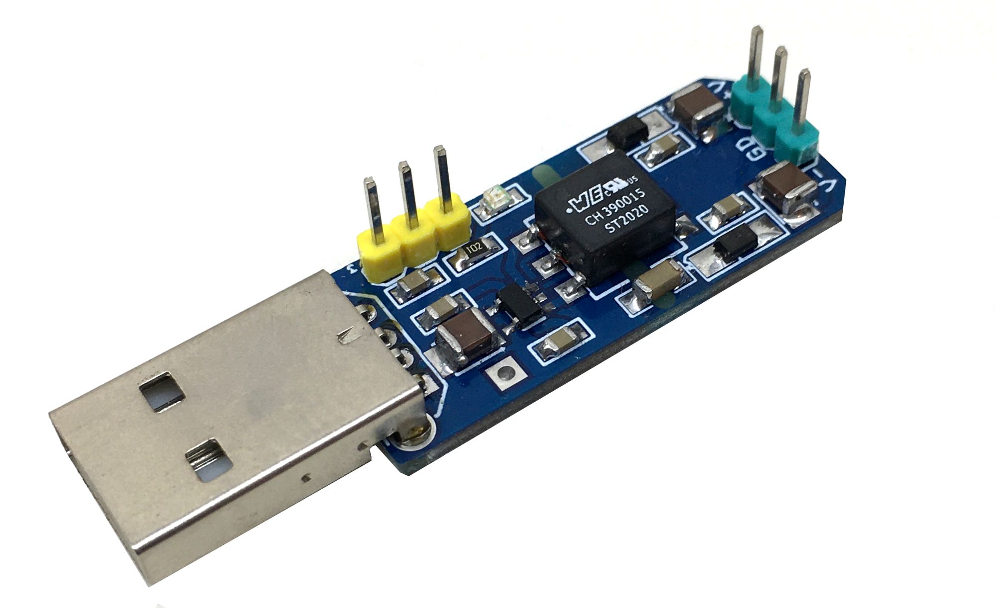
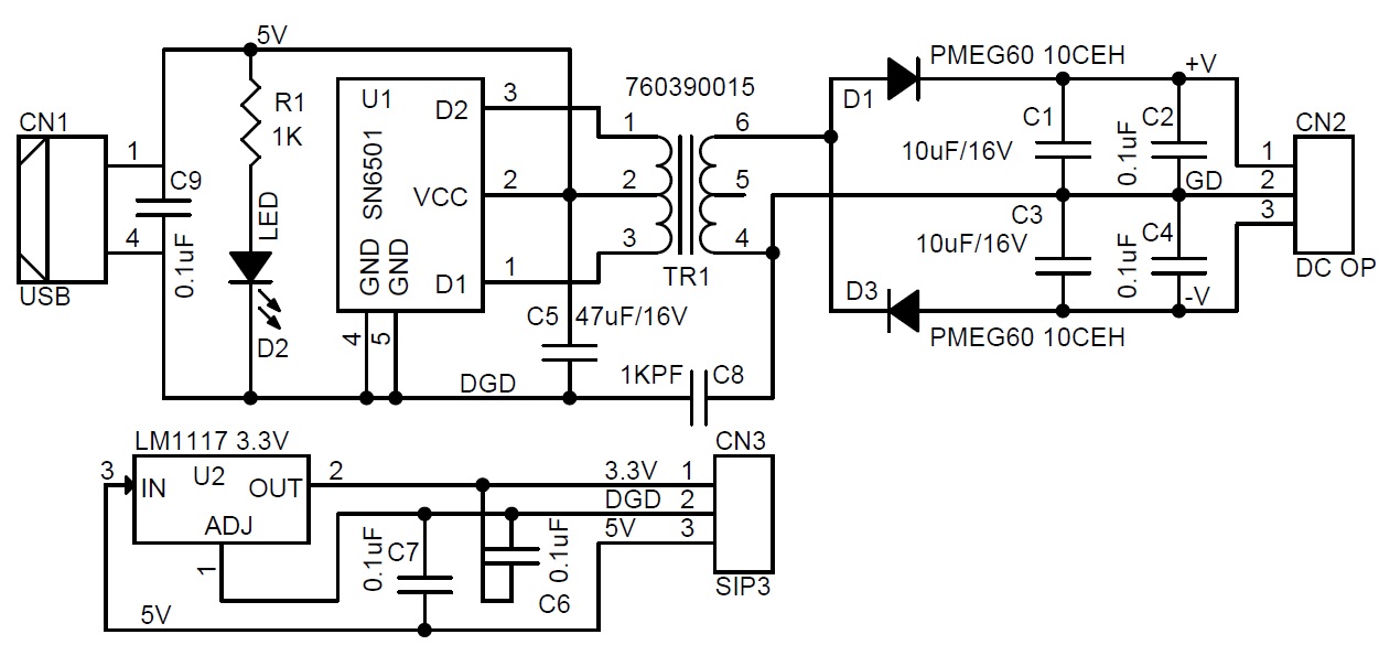
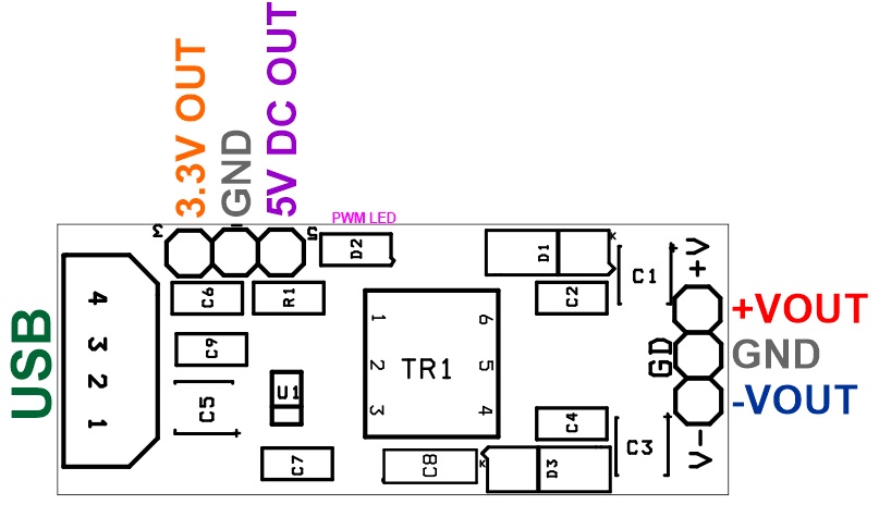
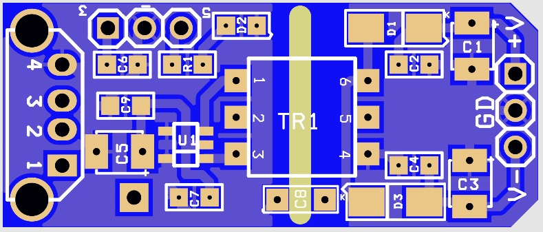
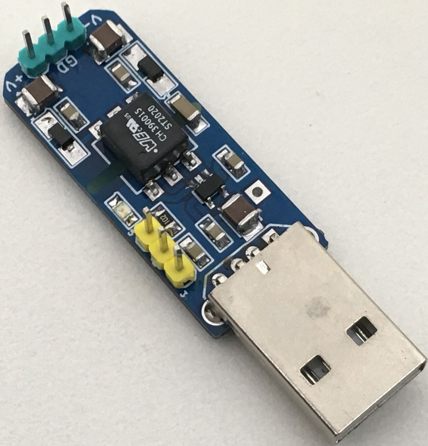
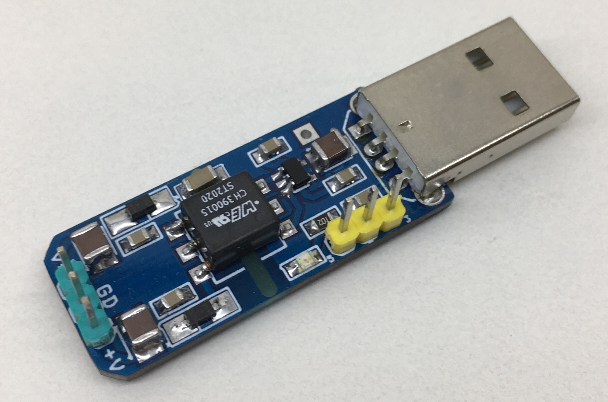
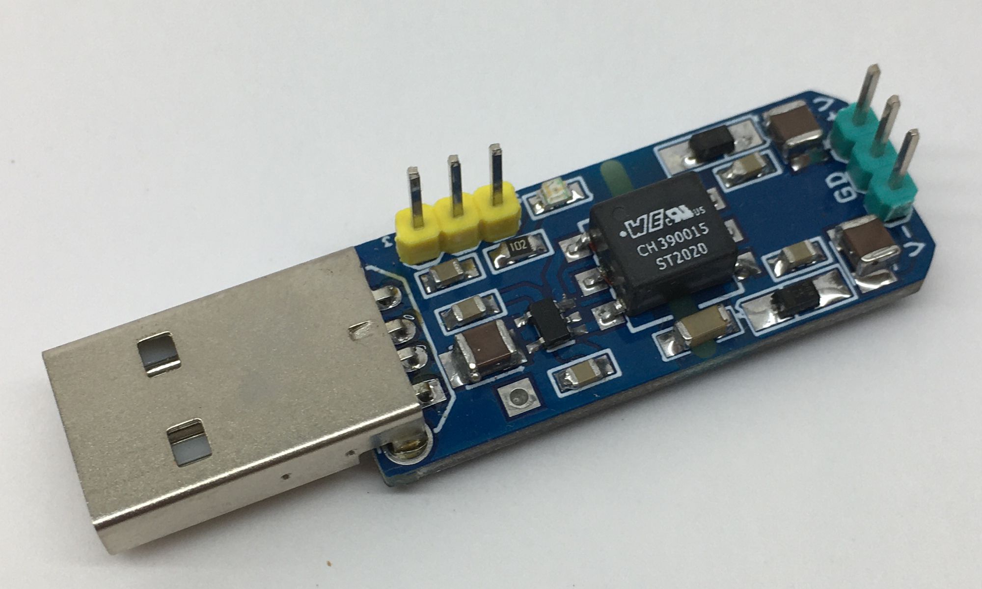
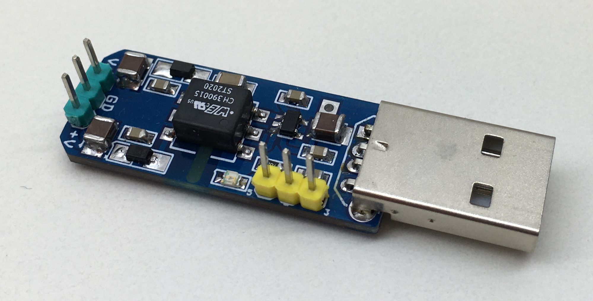
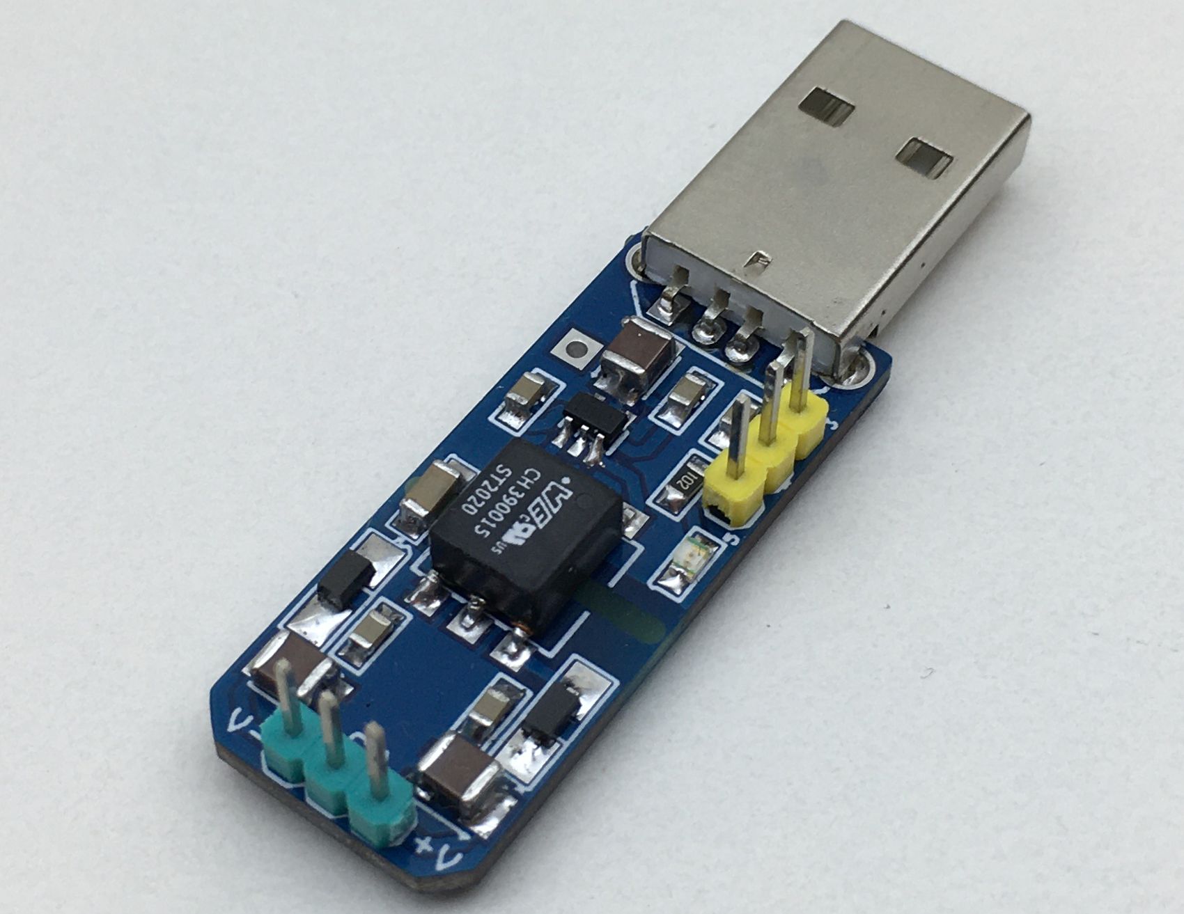
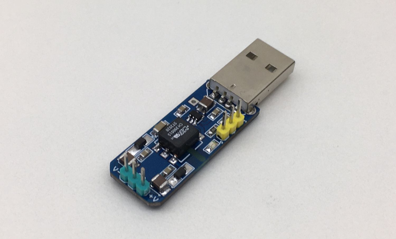
This is a mini DC-DC converter with dual output from single 5V DC supply or USB power source (e.g., +/-18V from 5V/USB). The mini board will fit into small space and perform with high efficiency. Basically, the circuit transfers power from 5V/USB to the output side +/-18V with high isolation, without a direct connection between 5V/USB power and output. The power isolation prevents ground loops and provides high noise immunity between input and output. The project is based on SN6501 chip, which is oscillator/power-driver, is specifically designed for small factor devices. The device drives a low profile, center-tapped transformer primary from 5V/USB power and secondary side provides unregulated dual output which can be further regulated as per requirement (e.g., +/-5V, +/-12V). Project is a very easy and simple tool to test and run industrial, scientific project, PLC and I/O modules which require dual output from single input. D2 power LED, CN1 USB A type connector for USB power input, CN3 No isolated 3.3V and 5V DC output, CN2 unregulated dual 18V Output.
The SN6501 is a transformer driver designed for low-cost, small form-factor, isolated DC-DC converters utilizing the push-pull topology. The device includes an oscillator that feeds a gate-drive circuit. The gate-drive, comprising a frequency divider and a break-before-make (BBM) logic, provides two complementary output signals which alternately turn the two output transistors on and off. The output frequency of the oscillator is divided down by an asynchronous divider that provides two complementary output signals with a 50% duty cycle. A subsequent break-before-make logic inserts a dead-time between the high-pulses of the two signals. The resulting output signals, present the gate-drive signals for the output transistors. As shown in the functional block diagram, before either one of the gates can assume logic high, there must be a short time period during which both signals are low and both transistors are high impedance. This short period, known as break-before-make time, is required to avoid shorting out both ends of the primary.
Features
- Input 5V DC @ 500mA (Power supply or USB Power)
- Output Unregulated +/-18V DC
- Output current 80mA (40mA + 40mA)
- Output 3.3V DC @ 150mA Non-Isolated LDO
- Output 5V DC @ 200mA Non-Isolated
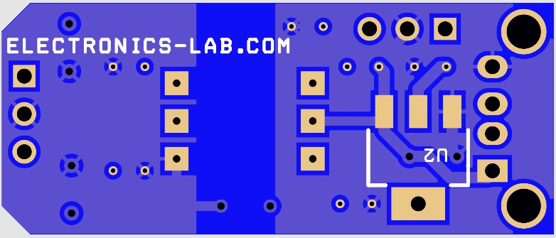
- PCB Dimensions 37.15 x 15.56 mm
Schematic
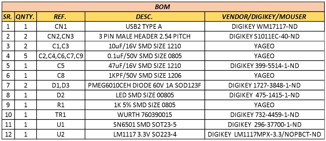
Parts List
Connections
Gerber View
Photos
I like this push-pull design,
(Is the C8 really needed ?)
I am looking for a similar design with output of +/-18V 0.4A each (14.4W)
(input 5V or 9V whatever is better possible)
do you have any ideas ?
The TI app schematics do not show C8. However, the output side isolated ground could get some common mode EMI from the
transformer switching.
It seems a little inadequate to place a 16V rated capacitors on the +/-18V outputs, no?
Is the module purchasable ? If yes then from where ?