Voltage to Current (V-I) Converter
The circuit shown here is a high-side voltage-to-current (V-I) converter. It translates an input voltage of 0 V to 2 V to an output current of 0 mA to 100 mA.
The circuit shown here is a high-side voltage-to-current (V-I) converter. It translates an input voltage of 0 V to 2 V to an output current of 0 mA to 100 mA. The low offset voltage and offset drift of the OPA2333 facilitate excellent DC accuracy for the circuit.
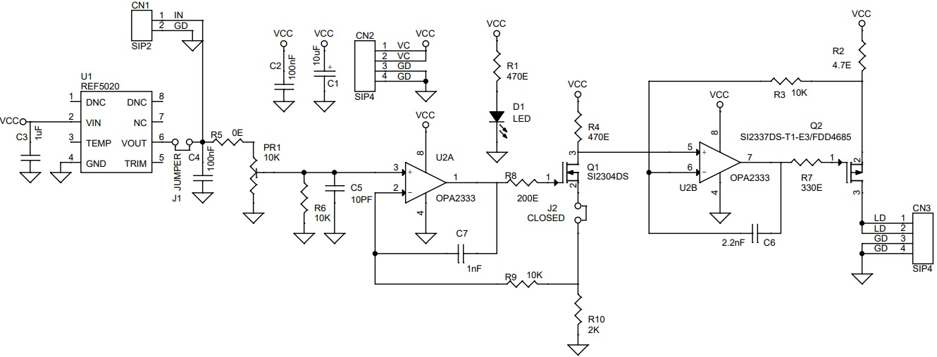
The project provides a high-side current source that supplies an adjustable current to a ground reference load. The first op-amp stage sets a reference current based on the input control voltage. The second op-amp stage acts as a current mirror that gains the reference current and regulates the current sourced from the output PMOSFET Q2 to the load. R2, R4, and R10 set the output current based on the input control voltage. Components C7, R9, R8, R7, C6, R3 provide compensation to ensure stability of the circuit.
The V-I transfer function of the circuit is based on the relationship between the input voltage, VIN, and the three current sensing resistors, R2, R4, and R10. The relationship between VIN and R10 determines the current that flows through the first stage of the design. The current gain from the first stage to the second stage is based on the relationship between R2 and R4. The project is built using OPA2333. Low offset voltage, low-temperature drift, and rail-to-rail output are the key features of this op-amp. The OPA2333 CMOS operational amplifier is a high precision, 5-uV offset, 0.05-μV/°C drift amplifier optimized for low-voltage, single-supply operation with an output swing to within 50 mV of the positive rail. The OPA2333 family uses chopping techniques to provide low initial offset voltage and near-zero drift over time and temperature. Low offset voltage and low drift reduce the offset error in the system, making these devices appropriate for precise DC control. The rail-to-rail output stage of the OPA2333 ensures that the output swing of the operational amplifier is able to fully control the gate of the MOSFET devices within the supply rails.
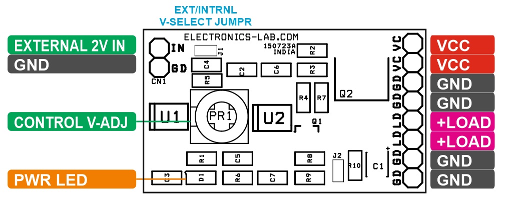
Control Voltage Input: The project works with external or internal control voltage.
- U1 REF5020 generates accurate 2V. Solder jumper J1 for internal control voltage, Trimmer potentiometer PR1 is provided to adjust the control voltage 0 to 2V.
- For external control voltage input, open the jumper J1, CN1 provided to feed the external control voltage 2V, PR1 can be used to adjust the 0 to 2V.
Features
- Input Supply 5V DC
- Input Control Voltage 0 to 2V
- Output 0 to 100mA
- Jumper For External/Internal Control Voltage Selection
- Reference Voltage Generator Chip for 2V Control Voltage Source
- Header Connector for Input and Output and Power Supply
- On Board Power LED
- On Board Trimmer Potentiometer for Control Voltage Adjustment
- Header Connector for External Control Voltage
- PCB Dimensions 36.83 x 20.96 mm
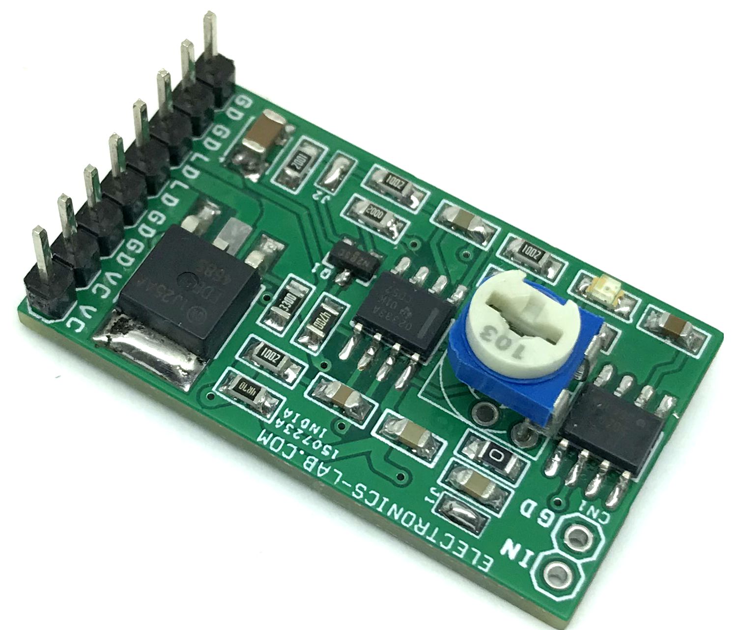
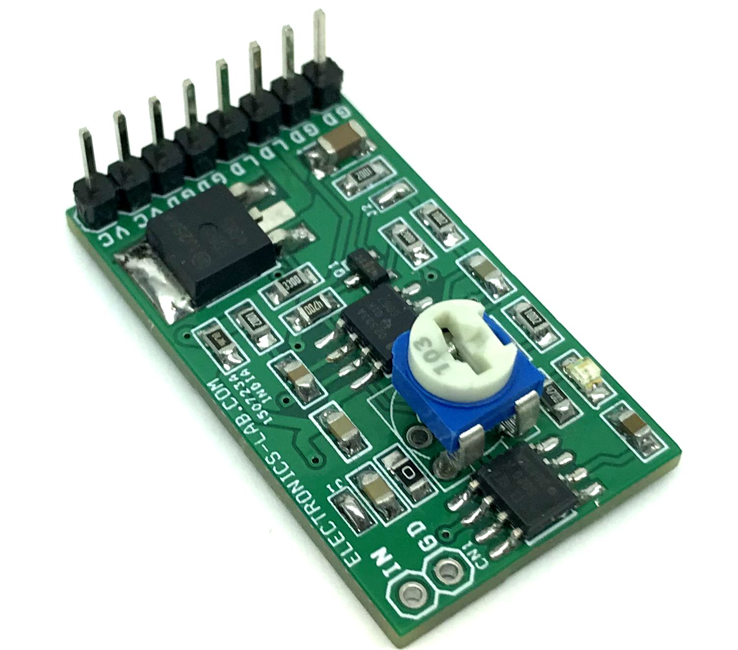
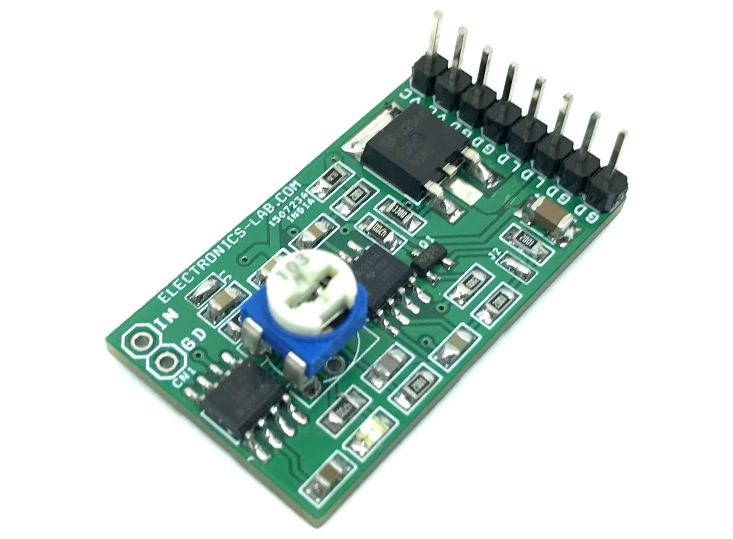
Connections and Other Details
- CN1: Pin 1 = 2V Input, Pin 2 = GND (External Control Voltage)
- CN2: Pin 1,2 = VCC, Pin 3,4 = GND
- CN3: Pin 1,2 = +Load, Pin 3,4 = GND
- D1: Power LED
- J1: Solder Jumper for External or Internal Control Voltage Selection. Open = External Control Voltage, Closes = Internal Control Voltage
- J2: Always Closed
Applications
- LED Drivers
- Optical Modules,
- Field Transmitters
- PLC Analog Output Modules
Schematic
Parts List
| NO | QNTY | REF | DESC | MAUFACTURER | SUPPLIER | SUPPLIER PART NO |
|---|---|---|---|---|---|---|
| 1 | 1 | CN1 | 2 PIN MALE HEADER PITCH 2.54MM | WURTH | DIGIKEY | 732-5315-ND |
| 2 | 2 | CN2,CN3 | 4 PIN MALE HEADER PITCH 2.54MM | WURTH | DIGIKEY | 732-5317-ND |
| 3 | 1 | C1 | 22uF/10V CERAMIC SMD SIZE 1206 | YAGEO/MURATA | DIGIKEY | |
| 4 | 2 | C2,C4 | 100nF/50V CERAMIC SMD SIZE 0805 | YAGEO/MURATA | DIGIKEY | |
| 5 | 1 | C3 | 1uF/25V CERAMIC SMD SIZE 0805 | YAGEO/MURATA | DIGIKEY | |
| 6 | 1 | C5 | 10PF/50V CERAMIC SMD SIZE 0805 | YAGEO/MURATA | DIGIKEY | |
| 7 | 1 | C6 | 2.2nF/50V CERAMIC SMD SIZE 0805 | YAGEO/MURATA | DIGIKEY | |
| 8 | 1 | C7 | 1nF/50V CERAMIC SMD SIZE 0805 | YAGEO/MURATA | DIGIKEY | |
| 9 | 1 | D1 | LED SMD SIZE 0805 | OSRAM | DIGIKEY | 475-1278-1-ND |
| 10 | 1 | J1 | JUMPER/PCB SOLDER | PCB-SOLDER | DIGIKEY | |
| 11 | 1 | J2 | JUMPER PCB/SOLDER | PCB-SOLDER | DIGIKEY | |
| 12 | 3 | R3,R6,R9 | 10K 1% SMD SIZE 0805 | YAGEO/MURATA | DIGIKEY | |
| 13 | 1 | Q1 | SI2304DS | NXP | DIGIKEY | 2156-SI2304DS215-ND |
| 14 | 1 | Q2 | SI2337DS-T1-E3/FDD4685 | ON SEMI | DIGIKEY | FDD4685CT-ND |
| 15 | 2 | R1,R4 | 470E 0.1% SMD SIZE 0805 | YAGEO/MURATA | DIGIKEY | |
| 16 | 1 | R2 | 4.7E 0.1% SMD SIZE 0805 | YAGEO/MURATA | DIGIKEY | |
| 17 | 1 | R5 | 0E | YAGEO/MURATA | DIGIKEY | |
| 18 | 1 | R7 | 330E 1% SMD SIZE 0805 | YAGEO/MURATA | DIGIKEY | |
| 19 | 1 | R8 | 200E 1% SMD SIZE 0805 | YAGEO/MURATA | DIGIKEY | |
| 20 | 1 | R10 | 2K 1% SMD SIZE 0805 | YAGEO/MURATA | DIGIKEY | |
| 21 | 1 | U1 | REF5020 SOIC8 | TI | DIGIKEY | 296-22201-5-ND |
| 22 | 1 | U2 | OPA2333 SOIC8 | TI | DIGIKEY | 296-19543-5-ND |
| 23 | 1 | PR1 | 10K TRIMMER POTENTIOMETER | PIHER | DIGIKEY | 1993-PT6KV-103A2020-ND |
Connections
Gerber View
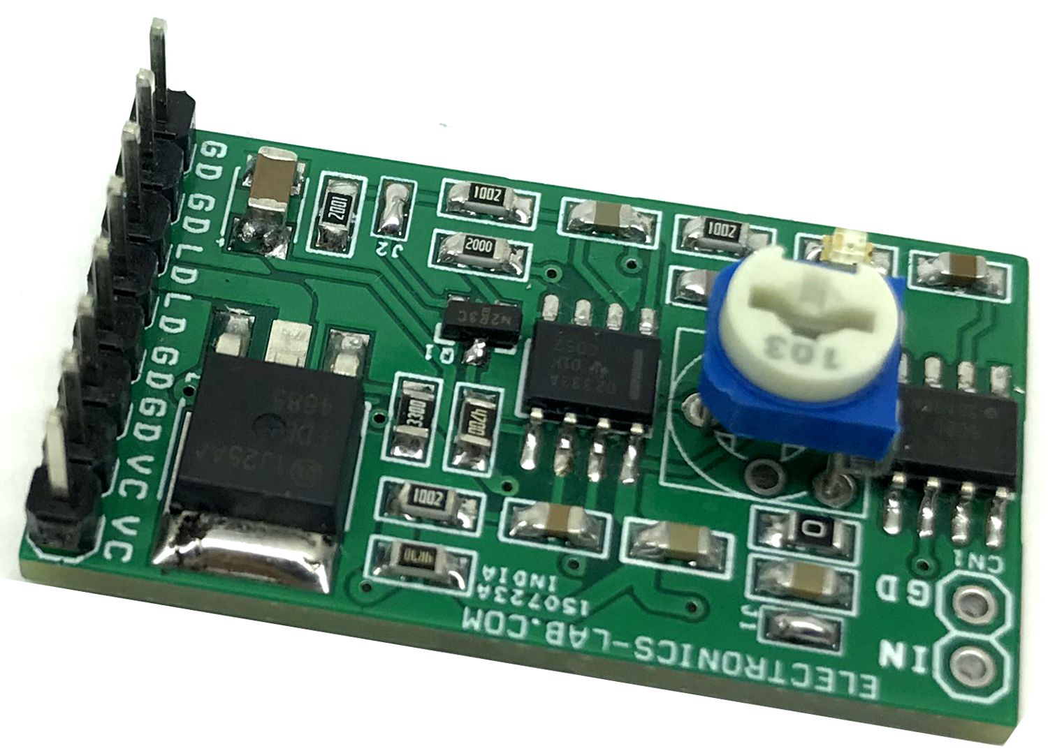
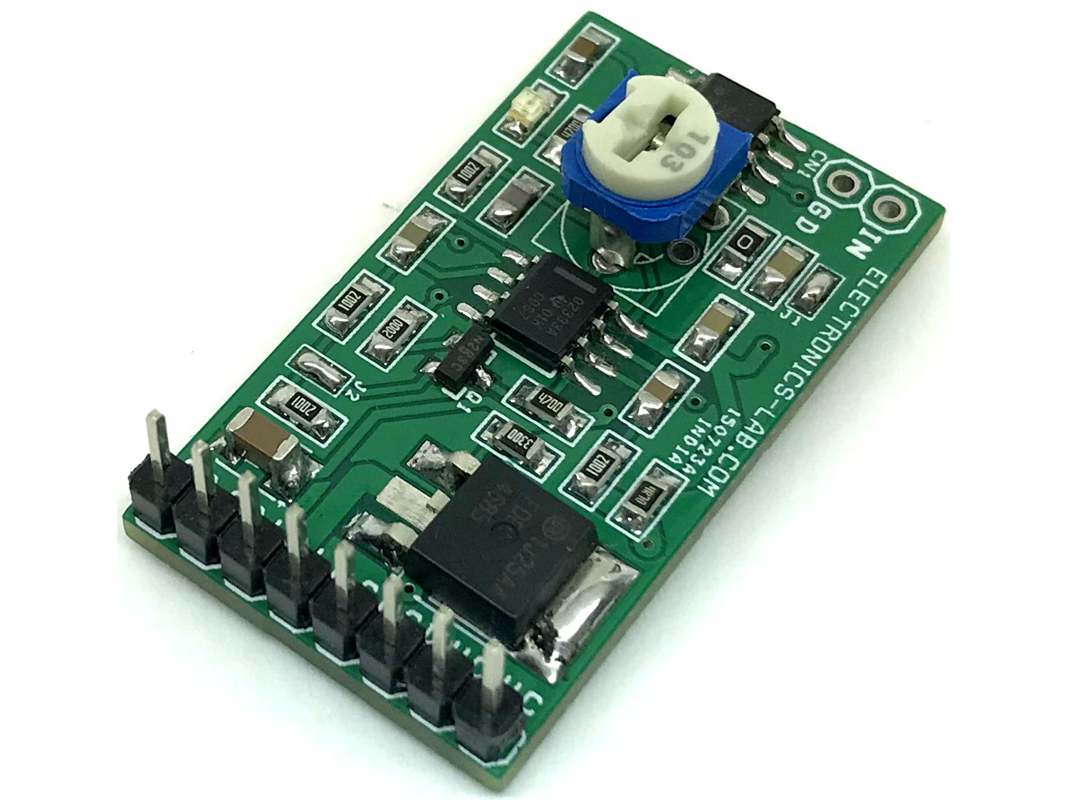
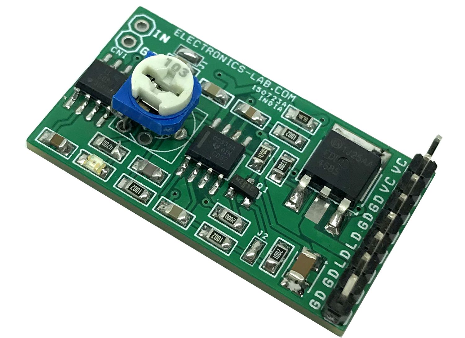
Photos