

Charger for mobile phones
- Izhar Fareed
- http://www.extremecircuits.net
- izhar@gmx.us
- 38.142 Views
- easy
- Non tested
- 0 Likes

Description
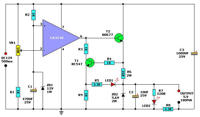
Most mobile chargers do not have current/voltage reguLation or short-circuit protection. These chargers provide raw 6-12V DC for charging the battery pack. Most of the mobile phone battery packs have a rating of 3.6V, 650 mAh. For increasing the life of the battery, slow charging at low current is advisable. Six to ten hours of charging at 150-200mA current is a suitable option. This will prevent heating up of the battery and extend its life. The circuit described here provides around 180mA current at 5.6V and protects the mobile phone from unexpected voltage fluctuations that develop on the mains line. So the charger can be left on over night to replenish the battery charge. The circuit protects the mobile phone as well as the charger by immediately disconnecting the output when it senses a voltage surge or a short circuit in the battery pack or connector. It can be called a middle man between the existing charger and the mobile phone. It has features like voltage and current regulation, over-current protection, and high- and low-voltage cut-off. An added speciality of the circuit is that it incorporates a short delay of ten seconds to switch on when mains resumes following a power failure. This protects the mobile phone from instant voltage spikes. The circuit is designed for use in conjunction with a 12V, 500mA adaptor (battery eliminator). Op-amp IC CA3130 is used as a voltage comparator. It is a BiMOS operational amplifier with MOSFET input and CMOS output. Inbuilt gate-protected p-channel MOSFETs are used in the input to provide very high input impedance. The output voltage can swing to either positive or negative (here, ground) side. The inverting input (pin 2) of IC1 is provided with a variable voltage obtained through the wiper of potmeter VR1. The non-inverting input (pin 3) of IC1 is connected to 12V stabilised DC voltage developed across zener ZD1. This makes the output of IC1 high.
After a power resumption, capacitor C1 provides delay of a few seconds to charge to a potential higher than of inverting pin 2 of CA3130, thus the output of IC1 goes high only after the delay. In the case of a heavy power line surge, zener diode ZD1 (12V, 1W) will breakdown and short pin 3 of IC1 to ground and the output of IC1 drops to ground level. The output of IC1 is fed to the base of npn Darlingtontransistor BD677 (T2) for charging the battery. Transistor T2 conducts only when the output of IC1 is high. During conduction the emitter voltage of T2 is around 10V, whichpasses through R6 to restrict the charging current to around 180 mA. Zener diode ZD2 regulates the charging voltage to around 5.6V. When a short-circuit occurs at the battery terminal, resistor R8 senses the over-current, allowing transistor T1 to conduct and light up LED1. Glowing of LED2 indicates the charging mode, while LED1 indicates shortcircuit or over-current status. The value of resistor R8 is important to get the desired current level to operate the cut-off. With the given value of R8 (3.3 ohms), it is 350 mA. Charging current can also be changed by increasing or decreasing the value of R7 using the I=V/R rule. Construct the circuit on a common PCB and house in a small plastic case. Connect the circuit between the output lines of the charger and the input pins of the mobile phone with correct polarity.


 Batteries")


Sir
My charger short circuited with a popping sound when it was connected to my phone..
After this incident, I am unable to charge my phone using any of the chargers…
What is the probable cause of this issue?
Probably your charging port or charging chip burned. You should bring your phone to a specialized mobile phone repair center.
What if i need 1A current or simply i want to built a 5v 1A charger what to modify in this circuit?
sir i want to make mobile charger of 400mA will you help me in choose of values of components used in it
This charger has a maximum output current of 180mA, for modifications please contact the author.
sir i know in train system is work on dc. but if i connect my charger ( mobile ) then how it can work.