redwire
-
Posts
244 -
Joined
-
Last visited
redwire's Achievements
")


-
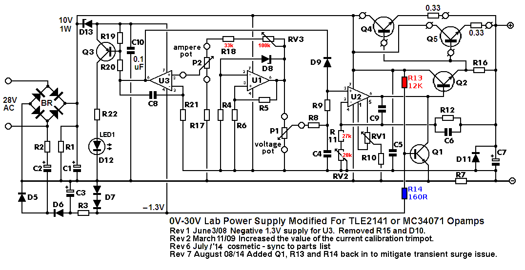
Dave, Can you provide a sketch showing the transistor layout between U1 and U3, as well as your modified the power supply to U1?
-
I'm planning to build (another) power supply with Q1 to see if it clamps down the output to prevent spikes when the power is shut down. I plan on using 7.5K and 240 ohm divider. With power on, the base of the transistor will be -0.03V. When the negative rail collapses, the base of Q1 will be 1.23V with approx. 5.1mA. Now I just need to pick out a good transistor for Q1.
-
I have a question about the sizing of the resistor divider for Q1 on the revised schematic. Currently it is listed as 12K and 160 Ohms. When the negative rail (-1.3V) is operating, the base voltage on Q1 will be approx. -0.7V assuming a Vdc of 39.6 on the top rail. When the power is shutting off and the negative rail collapses and goes to 0V, the transistor base will be 0.5 volts. The minimum on voltage for typical transistor( 2n2222) is 0.6V. Q1 will not have the minimum voltage to switch. Using a 12K resistor the current may not saturate the transistor to operate like a switch. The original design utilized a 5.1 zener for the negative rail with (10K and 1.5K) divider on Q1 resulted in a operating voltage on the base of the transistor of -0.01 V, but when the negative rail collapsed it resulted in 5.1V on the base of Q1. Do I have an error in my math?
-
 HaddyS reacted to a post in a topic:
0-30V 0-3A Latest Data Discussion
HaddyS reacted to a post in a topic:
0-30V 0-3A Latest Data Discussion
-
Thanks for the reply. I guess there is no getting around not having a negative charge pump with this type of design. I'm curious to see how this guy gets around the problem. Considering he is using a .1 ohm resistor, the theoretical load would be substantial before there would be stability. I think from a practical standpoint if there is a heavy load and 0.47 ohm sense reisistor, the ground for the current op amp is pushed low enough down to provide some control. I am also going to re-look at the design on the first post here. I seemed to have the oscillation under control and I could change the voltage smoothly. I was having some current control issues in that the opamps seemed to be fighting each other until the current setting was set to its lowest setting. If I set the voltage at 14V and the current at 100mv, then connect a load of 1.5 A the current control would never kick in. It was like in a runaway mode.
-
Here is the sketch with the diode on Pin 3 to compensate for the diode drop on the current op amp. Would this work?
-
Yep, your right. could you add another diode on Pin 3 of the Voltage op amp after the other diode leading to the current op amp. This way the voltage set for 0 V output is actually 0.7 on the line leading to the non inverting pin. Then the current op amp would only need to bring pin 3 the line down to 0.7? .
-
Yes I did forget to show the diode from pin 3 on the voltage Opamp to prevent positive voltage from the current op amp. The op amp (TLE2141) can handle 0-44V and sink up to 80ma. I estimate there will be no more than 8ma to sink on the current opamp and about 3ma output on the voltage op amp using the darlington transistor.
-
How about this redesign ? Circuit_II.pdf
-
Another question: Is the 100K resistor base resistor for Q2 (2n2222 voltage control transistor) really necessary?
-
Would using a voltage divider from the output of the Opamp to the 2N2222 allow a significantly lower base resistor and reduce the phase shift? Would a different transistor also help?
-
This is not a revision of the Power supply with 163 pages. This is a different design based on the original circuit here. Which was posted on Youtube here Although I changed some values I did not add any transistors or reconfigure the basic circuit design but I did add some caps for the op amps which gives is a design that appear to be similar to the long posted design. Regarding high gain, if a BJT transistor is current driven wouldn't reducing the current by adding a resistor to the base also reduce the gain and negate the effects. I found with a 10k resistor on the darlington MJ11016 and a 1.2K with the 2N5886 the oscillation ceased. I found I still needed at least a 47uf cap so I decided to keep the 100uf. So far I have gotten no other recommendation to attack the phase shift issue except redesign.
-
But I didn't add another driver transistor unless you are referring to the use of the MJ11016 darlington output transistor. I did try the circuit with a 2N5668 and it had the same output problems. The original design used a 100uf cap at the output. Initially I thought this was too high and changed this to 10uf like the other design when I had oscillations I changed it back to 100uf, but now it seems I was heading in the wrong direction and need to change it back to 10uf. It seems having a slow output tranistor with a fast opamp can be an issue. So would using a faster power transistor help? If so, how do I choose a faster transistor from the data sheet, by the bandwidth product? a 2N3055 is listed at 6MHz, but a 2N3442G is listed at 80mHz. Would that help? I added a 100k resistor to the base of the MJ11016 power transistor and the oscillations did stop. I will change the 100uf cap back to 10uf . I didn't like the response on the current control and the setup with the led connected directly to the output of the opamp concerns me. It seems this indicator should be driven by a transistor. I noticed that when the inverting pin was higher than the non inverting pin the output voltage on Pin 6 would slowly decrease (over seconds) instead of nearly instant control. I may need to change C4 to 100pf instead of 220nf but I don't see that as a total fix becasue of how slow it is responding.
-
Would adding a resistor to the base of Q1 (BD140) and to the base of the power transistor be a solution? What about changing to complimenary transistor set up (BD139) with a lower gain rather than the 2N2222 which has a much higher gain?
-
The other thread seems to be corrupted or locked so I will continue here Although I had many wires and jumpers the PS seemed to work well and testing seemed good until i shorted the board and burned some traces. Happy with the design, I had 3 new boards made and populated 2 of them. Unfortunately something is not right. When there is no load, the voltage would spike up and down about once a second. If I disconnect the feedback from the power transistor to the board it will not spike. I changed C5 from 100pf to 200nf and the output was steady without a load. If set the voltage to 4V and connect a load, the output shoots up and oscillated between 35V and 17V at about 800Hz. The voltage and current regulation did not seem to work. Only if I set the current to minimum and then apply a load it will not spike and oscillate. I changed the output tranistor from the darlington to a 2N5886 and had the same results. Any suggestions.
-
Looking for suggestions. I built the board as shown in the above post with quite a few wires and jumpers and things seemed to work very well. I then had 3 boards made. I populated 2 of them. Strange things happend on the new boards. With no load the output would spike about once every second. I changed C5 to 200nf instead of 100pf and the PS worked smoothly with no load. If I set the voltage to about 4V and connect a load, the output voltage instantly surges and oscillates between max and 17v at a frequency of 800hz. Neither the voltage or current control seem to work with a load. If I set the current to minimum before attaching a load then the PS will not ramp to max and oscillate.