
.png.b1e42692bc15eb316aa8208359d74f30.png)
Aman bharti
-
Posts
31 -
Joined
-
Last visited
Content Type
Profiles
Forums
Events
Posts posted by Aman bharti
-
-
Sample and hold circuit
Definition and Introduction
Sample and hold circuit is an electronic circuit which makes the samples of input voltage signals and holds these samples signal for some very small time duration.
Sample and hold circuit is basically is an analog to digital converter circuit. Input voltage signals to be sampled and hold for some duration (in microseconds) using the capacitor and give the output in the form of digital pulse. Because this works by the holds the sampled analog input signal this is called the sample and hold circuit. Holding of the signal is done using a capacitor called holding capacitor, capacitor has the ability to store the voltage by charging until it will discharge. This charging and storing property of the capacitor is used here for the holding of the signal.
Sample
Some Parts consider or Take the values of a given continuous input signal at each different time is called sample.
Hold
catch the sampled signals and take hold for a time t is called hold.
Sampling time
The time during which generates the samples of input signals called sampling time. This is usually 1us to 14 u sec.
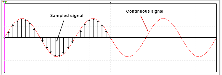
Holding time
The time during which the circuit holds the sampled value is called the holding time. Holding time to be set according to the required for application.
Basic sample and holding circuit
A basic sample and hold circuit consists a switch and a capacitor. A combination of a control switch and a capacitor is called a simple sample and hold circuit. Input voltage applied at the point Vin and then a switch connected after that a capacitor connected between the switch and output. One side of the capacitor is connected with the ground. A JFET or a MOSFET is used as a Control switch.
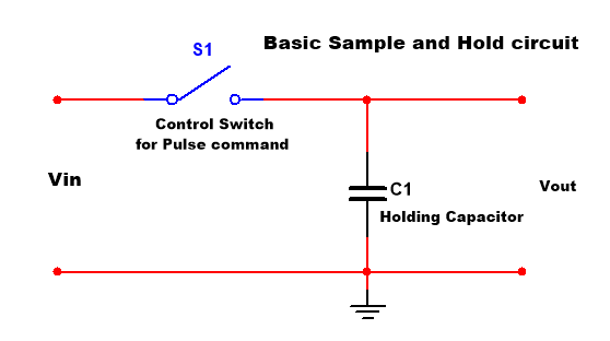
Working
When the switch is closed the connected capacitor charged and when the switch is opened the capacitor will not get discharged because there is no path for discharging and then the capacitor takes to hold the signal.
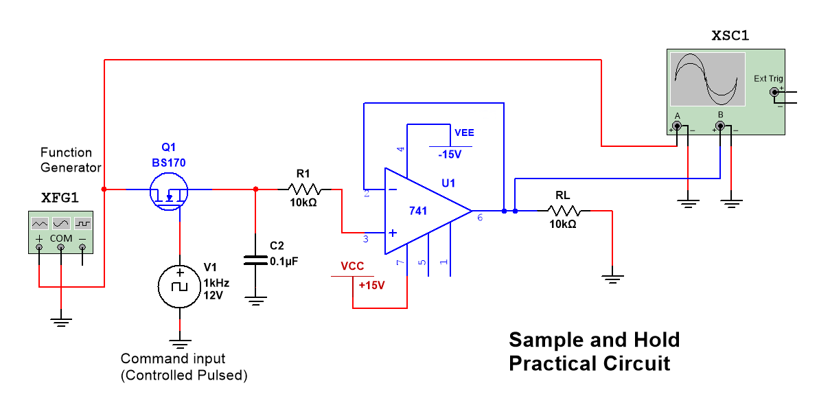
Sample hold circuit using op-amp
In this circuit two voltage follower circuit, a capacitor and A MOSFET connected. Input voltage given at The control voltage is given on the gate terminal of MOSFET, here MOSFET is used as a switch. The reason of using the Voltage follower circuit is this circuit gives output same as the input signal and there is a very high input impedance so no load is considered at the input and the capacitator will also not get discharged because of very high impedance at the input of the op-amp.
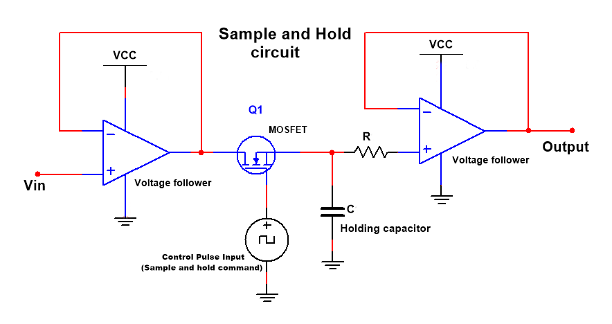
The MOSFET is used here as the control switch for applying the voltage pulse. The Gate terminal of MOSFET is connected with a controlled pulsed signal generator. Astable multivibrator can be used to produce frequency. This astable frequency switch ON-OFF Very fast the MOSFET. By the ON-OFF, ON-OFF of the MOSFET a pulsed form of the input voltage signal is applied to the NON-Inverting terminal of Op-amp. The capacitor will charge as a pulse signal gets for the 1st pulse to its max level and this level is HOLD for a definite time by the capacitor because this capacitor will not discharge. And now the next pulse falls and the capacitor will again charge as this pulse voltage level and this level hold and this process is continuously proceeding as per pulse signal and the amplitude level of the pulse signal.
So, in this whole process, the output is sampled and also hold for a time duration, these are done by the main capacitor used in this circuit. We know that the sampled signals are the digital signals, So we can say that the sample and hold circuit converts analog or continuous-time signal into digital signals.

Uses or applications of Sample and Hold circuit
- ADCs (Analog-to-Digital Conversion)
- DACs (Digital-to-Analog Conversion)
- In Analog Demultiplexing
- In Linear Systems
- In Data Distribution System
- In Digital Voltmeters
- In Signal Constructional Filters
more articles on www.circuitspedia.com/
-
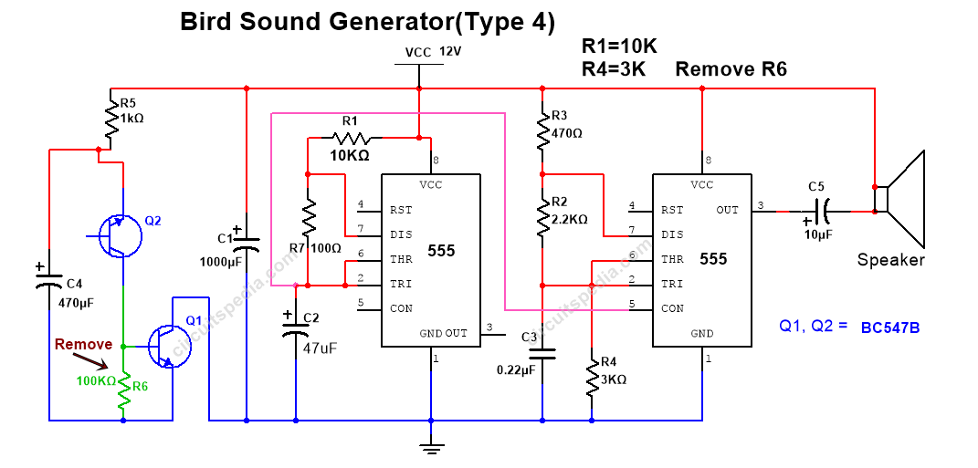
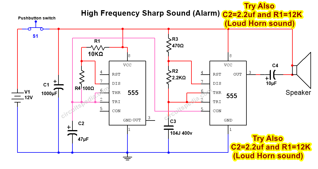
Tone generator circuit using 555 timer
Bird sound generator, Ambulance Siren Generator
These are some circuit diagrams of the sound generators. Sounds are like Bird sound, Ambulance siren, Beep Horn, and other different types. Use 9 to 12v Dc supply and components value should be the same as suggested in the diagram because any variation of components value can change the sound type.
By some changes of values of some components as given below in the diagram, you can produce many different type of sounds. Use a medium-size speaker, These circuits can be useful for the making of Alarm, Doorbell or other warning indicators.
For more circuit diagram go to circuitspedia.com
Testing Video
Also read
-
why ac current passes through capacitor but dc can’t
how capacitor block dc current
Explanation 1
We try to understand using a discharged battery in the circuit. When switch on, the battery is starting to charge and increasing the voltage level of the battery and there is a flow of current.
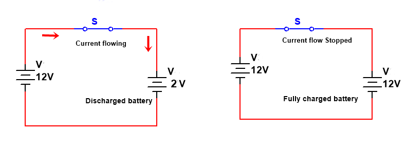
When the battery gets fully charged and the voltage of a battery increase and is equal to supply voltage then there is no flow any current between them.
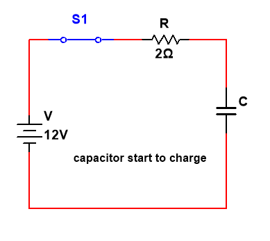
Let us consider a simple circuit as given below. In this circuit, a capacitor is connected with a resistor in series. A 12v DC power supply is used. This circuit is open because the switch of this circuit is open.
In the case of capacitor If I turn on the switch then what will happen? After the supply used in this by turning on the switch, the Capacitor will start to Charge and this capacitor will charge continuously till the voltage is equal to supply voltage. Here 12v used so capacitor is getting charged from 0v, 1v, 2v,3v,4v……….upto 12v. And when capacitor charged with 12v then it will stop to charge. If supply is used of 9v then the capacitor will stop to charge after 9v.Now, we take a look at the following diagrams.
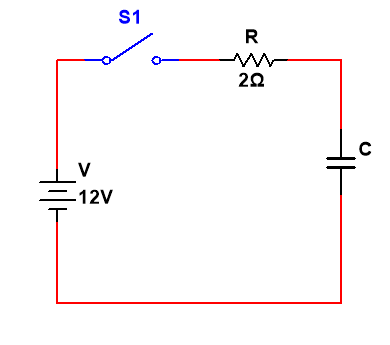
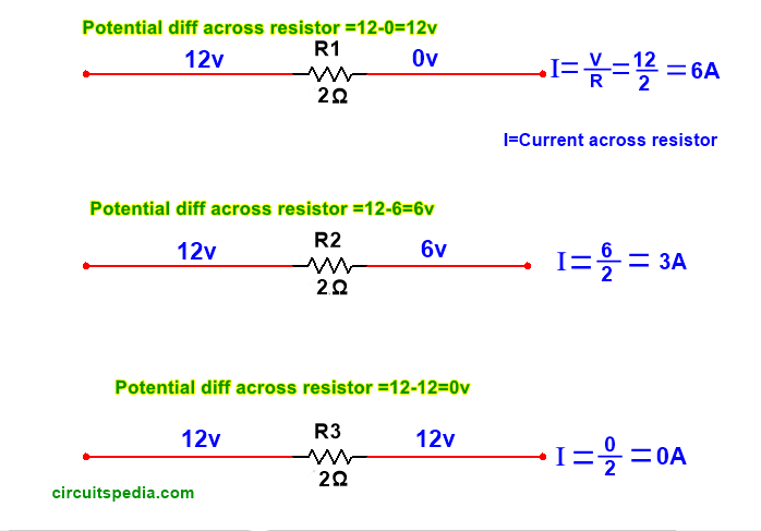
A resistor of 2 ohm is in the diagram and one side of the resistor is voltage is 12v and the other side is 0v. So here is the potential difference between two points is 12-0=12v. Means voltage across the resistor is 12v. So the current conduction is I=V/R=12/2=6A. If other side voltage increases and becomes 6V then the potential difference is 12v – 6v=6v means voltage across the resistor is 6v. The current conduction is I=V/R=6/2=3A. So we see here if the voltage at the two-point in the circuit has much differed then the potential difference between them is high means the voltage level is high and there is high current flow. But if the voltage at two points in a circuit is Similar then the potential difference between them is 0, so the voltage is 0 between those two points. In this case, the current flow is 0/2=0A, which means no current flows.
The same phenomenon occurs with the Capacitor. At starting when the Capacitor starts to Charge from 0v, A current flows through the capacitor in the circuit. But after some time when the capacitor gets fully charged and the voltage level of capacitor increase maximum or equal to supply voltage, then there are 0 potential differences and then no current flows across a capacitor.
In the diagram, we see that the voltage level is equal to both sides of the resistor after a full charge of the capacitor, so there are no current flows across the Capacitor because of the potential difference across it become 0v.
Actually capacitor doesn’t block DC current, the capacitor makes potential difference high to very low (about 0) and stops the current flow between them at a particular portion of a circuit by itself charge. But we feel like the Capacitor block DC current.Explanation 2
When switch on supply then Electrons start stored in the Capacitor and after some moments capacitor gets charged by Electrons and positive ions. After charging the Capacitor Electrons are repelled by charged Electrons and then the capacitor works like an open circuit.
As formula Xc=1/2πFC
In DC there is no frequency so F=0. So Xc=1/0=∞.means there is very high resistance across the capacitor. So in dc capacitor acts as an open switch after charge.
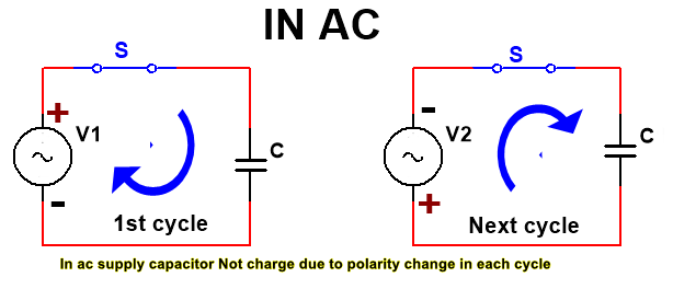
In AC current there is frequency. So continuous changes in polarity between negative and positive and this reason capacitor don’t get charged. In ac, the capacitor acts as a short circuit.
As formula Xc=1/2πFC
In AC always some value of F. So always a reactance creates across the capacitor that allows flowing the current.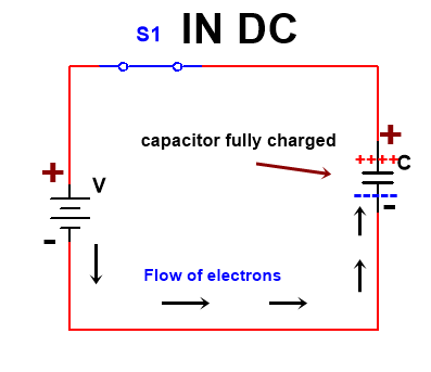
Also read-
Flip-Flops, S-R and J-K Flip flop
.
-
Comparator
A comparator is a circuit that compares two input voltages or currents and gives output High or Low as per input signal. The Output is a digital form according to the input signal compared with the reference. Basically a comparator is used in electronics to compare the two Analog input signals given on both input terminals and we get the Digital output as High level or Low level.
Comparator is used to sense the signal of a predefined rich level. If I set a level to sense then I can use a comparator to sense it when the input signal of this level cross more or below the level, suddenly the output is changed from Low to high and high to low. The comparators are used for so many electronics instrumentation for automation and drive different logic circuits.
Difference between operational amplifier (op-amp) and comparator
The symbol of the operational amplifier and comparator are looked the same. But Op-amp is designed to accept an analog input signal and also give the output Analog signal. But the Comparator accepts the analog input signals but gives the digital output. Comparators are faster than the operational amplifier. An op-amp will works as the comparator if using the transistor at the output.
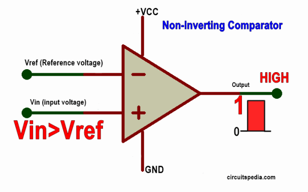
If the input is applied at the + pin, this is called non-inverting input
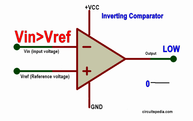
If the input is applied at the – pin then this is called the inverting input
Non-inverting mode
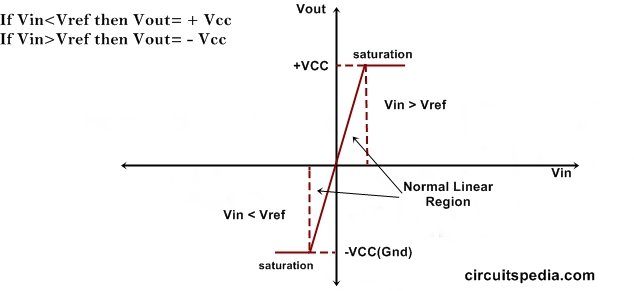
If I connect the input voltage at the non-inverting input and set a reference voltage level at inverting input which is to be sensing. In this circuit, the voltage will compare with the reference. If the applied voltage is lower than the reference voltage then the output is LOW, and if the applied input voltage is greater than the reference voltage then the output will HIGH. Here High level means output is directly connected automatically with VCC and Low means Output is directly connected with Ground.
For example, if we set the reference voltage at 6v, then when the input voltage increases to 6v then the output suddenly swings to HIGH and gives the voltage the same as VCC, Otherwise output gives the LOW or 0v voltage.
Input voltage > Reference Voltage – Output HIGH
Input voltage < Reference Voltage – Output LOW
 comparator circuit diagram
Inverting Comparator
In inverting mode the input voltage is connected with the Inverting terminal and reference voltage is st at the non-inverting terminal. In this connection, the voltage at the Inverting terminal will be sensed and compared with the voltage at the non-inverting terminal which is the reference voltage. The inverting mode comparator works reverse to the non-inverting comparator. Means If the voltage at Inverting terminal is greater than the Reference voltage then the output will LOW, But If the Input voltage is Lower than the Reference voltage than the Output Will HIGH. This comparator gives output Inverted of input.
For example, Reference voltage adjusted at 6v, when the input voltage increases and goes to 6v then the output will suddenly swing to LOW or 0v. Otherwise, the output will HIGH and give the voltage the same as VCC.
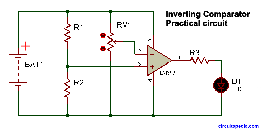
The LM358 is the very popular comparator ic used for general purposes. This ic has 2 opamp comparator. LM324 is also a very popular and most using comparator ic. It has quad op-amp comparator.

Also Read Kirchoff's Law
.
-
What is ohm’s law
In the electrical field, Ohm’s law is a very important topic. This law is asked in almost all interviews and as basic fundamentals of electrical engineering for all who related to electrical engineering. This is a very important fundamental law that describes the Relation between Current, Voltage, and Resistance.
There are three main quantities present in Electricity. An electrical circuit is made by these three Quantities Current (I), Voltage(V), and Resistance(R). There is no imagine the electrical circuit without anyone thing of them. And one other essential quantity is Load. Because the current is flowing only if there is any load connected with the circuit.
Ohm’s law is given by a German mathematician George Simon Ohm, who formulated the law known after his name as Ohm’s law.
Also read Thevenin Theorem
Ohm’s law definition
Ohm’ law states that if physical conditions (like- temperature, pressure, length, etc) are constant, then the voltage across the two terminals of conducting material is proportional to the current flowing through it.
Ohm’s law formula
Ohm’ law is expressed as V∝I
In the given fig when we connect a battery across the conductor then an electric field E is created and electrons move to the reverse direction of the electrical field.

If I consider a cross-sectional area in a conductor, Then the number of total charges passed across a cross-sectional area in one second, which is called Current in the conductor. Now if I increase the potential difference across the conductor, The electric field and magnitude are also increased and the forces of electrons are also increased and the magnitude of electrons is so increased. Now the all free electrons will move with more speed. That means the number of electrons that were crossed across the cross-sectional area will now be increased and a large number of electrons cross across the cross-sectional area of a conductor in one second. And we can say that the current is increased across that cross-sectional area.
If the potential difference increased by doubled then the current will also be doubled and the potential difference is increased 3 times then the current will also be increased by 3 times. so we can say that the Voltage (potential diff) is directly proportional to the current (I). V∝I if we replace the proportionality sign by = we need to place a constant. here R is the constant of proportionality that can be placed here. So V= I.R, R is resistance. Means R is in the circuit provided R is kept constant. Resistance is a fixed quantity of a particular conductor.

But if i change the conductor material then the Resistance will also be changed. Also when I changed the length or thickness of the conductor then Resistance will also be changed.
V is the s.i unit of potential difference and Ω is the s.i unit of resistance. And I is the si unit of current. Ohm’s law is used to find the current, Voltage, and Resistance in a circuit.
How we use the ohm’ law
For example, in the given diagram a 9v battery is directly connected with an LED. This Yellow LED works with the 3v (only for example actual voltage for the yellow LED may different) and 20ma current, But in the diagram, the applied voltage is higher than required. If I give more power than this the LED will burn as shown in fig. So I need to drop the voltage and current as suitable with LED.
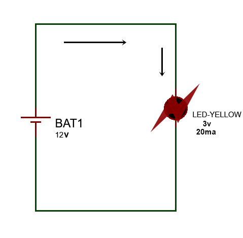
Given
LED voltage = 3v
Supply voltage = 12v
LED current = 20ma
We need to drop the voltage for LED = 12-3 = 9v, It means we need to reduce 9v from 12v battery. So Take here V= 9v,
Then V = I.R
20ma = 0.02A (1A=1000ma)
9= 0.02 . R, and R = 450Ω, It means we need to add a minimum of 450 Ω resistor with the LED for Proper working.

This Relationship between current-voltage, Resistance is not apply to all non-metallic conductors. It does not apply to non-linear devices such as Zener diodes.
Must Read What is comparator
.
-
On 9/20/2018 at 9:20 PM, audioguru said:On 10/1/2018 at 11:30 PM, ELECTROMAGIX said:
 On 10/1/2018 at 11:30 PM, ELECTROMAGIX said:
-
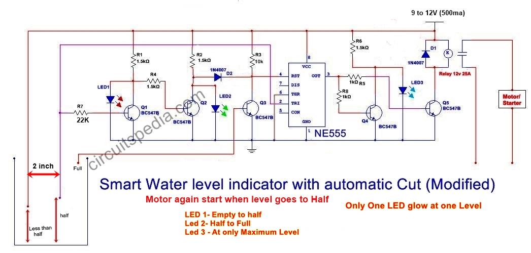
you connect the circuit before the starter, i mean the supply to the motor starter pass through this circuit Relay.
You start the motor using start switch ,when tank will full, then automatic stop the motor.
-
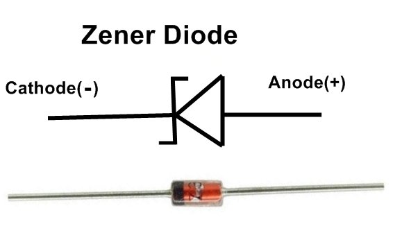
Zener diode working
Zener diodeZener diode is a type of diode which flow of current also in reverse bias and in applications it always connected in reverse bias and zener diode limit the voltage, this diode is used for regulating the voltage in any circuit. It always works in zener breakdown voltage. Zener breakdown voltage is voltage level at this zener diode starts the current conduction in reverse bias. When reverse voltage increases then current conduction starts at a level, this level of voltage called breakdown voltage and the current flowing through diode is called zener current. This process is called avalanche breakdown .
First we take a look on normal diode . A normal diode works only in forward bias, means voltage on cathode is less than anode . Voltage on anode is high with respect of cathode then it is called forward bias, in this condition a norml diode starts conduction. If voltage on anode is 2v and voltage on cathode is 0v or voltage on anode is 5v and 2v on cathode then conduction starts and diode will work , but if voltage on anode is 0v and voltage is on cathode is 2v then normal diode will not work and this is called reverse connection.
In reverse bias after a limitation of current flow barrier break and a reverse current flow
A normal diode only work in forward bias . If we give voltage more than breakdown voltage in reverse bias in normal diode then it will damage permanently. This drawback of normal diode removed in zener diode . A zener diode work as normal diode If it connected in forward bias . But zener diode also conducts current in reverse bias connection with specified condition.
zener diode as voltage regulator
We try to understand how zener diode works and regulate the voltage.
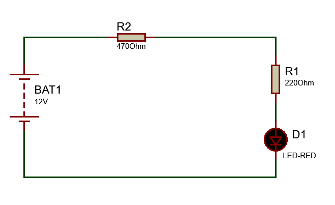
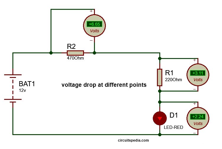
V1 (BAT1) is a DC source , a load is connected and denoted as RL, a zener diode is connected across the RL through a resistor . In this circuit anode of zener diode is connected with negative terminal of battery and cathode of zener is connected with positive point of battery. So this connection is in reverse bias. 12v DC source or battery applied and R1 is 220 ohm , R2 is 470 ohm and an LED is connected with R1 as Load.
Now we check the voltage at all resistors and load, voltage are divided at all resistor and load according to resistances at each point as divider formula. I connect three DC voltmeter at each resistor and load to measure the Voltage Drop at each part. As you see in the circuit diagram given Voltage drop across R1 = 3.114v, across R2= 6.65v and voltage drop at load (LED)=2.24v. so, 3.11v+6.65v+2.24v+6.65v=12v
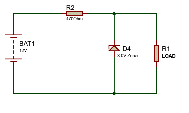
In this circuit arrangement the Total voltage across the load is 2.24v (Here load is LED). If i want to voltage at load load fix 3v But input source voltage remain 12v, then what should i do ?
zener diode circuit
Also read Logic gate concept
For 3v output we should connect a 3v zener diode to parallel with output load . One thing is noted here that a resistor must connect before the zener as series with positive voltage . But here is a Question about this resistor , Why use this resistor ?
Why do i connect a resistor with zener diode ?


When we connect zener diode at output in reverse bias , then current through diode pass according to the source voltage. Here source voltage is 12v that is fix . If the source voltage increase then the current conduction through zener diode also increases and extra voltage drop at the resistor R2. If the source voltage vary then the current conduction through zener diode and resistor also vary and all varied extra voltage will drop at resistor R2 and we found a fix regulated voltage at output. So all extra voltage will drop at resistor that is connected in series with zener. It means according to applied input voltage increases, the zener diode allow to pass more current through itself by the series resistor therefore the current conduction through resistor and zener diode increase as per input voltage, and the point of zener diode we get regulated fix voltage as its rating.
If you need 3v output then use 3v or 3.1v zener diode and according to if you need 5v then use 5.1v and 9v fzener for 9v output 12v zener for 12v output.....But applied input voltage Must higher than required output voltage because zener diode always works in breakdown region so for breakdown the applied voltage should higher than the breakdown voltage.
There are limitation of current conduction capacity of each zener . Zener diode available in market at the rating of different watt with different voltages.
The value of series resistor can be determined by using following given formula
R=(Vin -Vz)/Iz
Where R= Series resistor
Vin= Applied input voltage
Vz= Zener voltage (this is equal to Output voltage V0)
Iz= Zener current
Also read Active, Passive,Linear,Non-Linear ,Unilateral element etc
-
Semiconductor P-N Junction Diode Working Principle
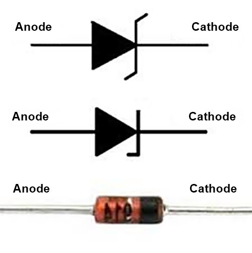
Diode is the two terminal polarised electronic semiconductor device . One terminal is Anode(-) and other is Cathode(+). The cathode is marked with the silver colour or colour band. This is the simplest semiconductor device but this is very important and most useful in electronic circuits.
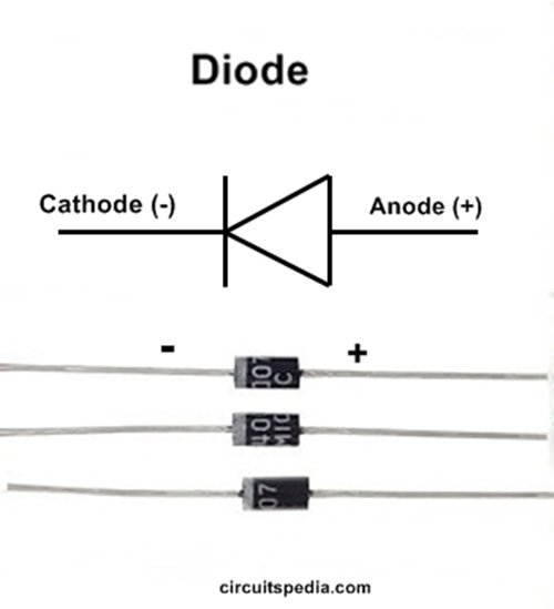
Diode Function
The main function of the semiconductor diode is the flow of electrons to totally in only one direction across it . It means Diode conducts current in only one direction. If change the polarity of diode then no any current passes through it. So we can say that diode is act as a switch which allow to conduction of current in only one direction. This is property of an Ideal Diode.
An Ideal diode acts like short circuit with same polarity with supply, But in Reverse connection it acts like Open circuit means no any current flows in reverse polarity.
The semiconductor Diode is formed by adding and apply a burning force or crystalization on together of P-type and n-Type materials (p-n junction). Joining of Both materials should of the same base - Ge or Si. The PN-junction is the basic root for semiconductor diodes .
 PN junction
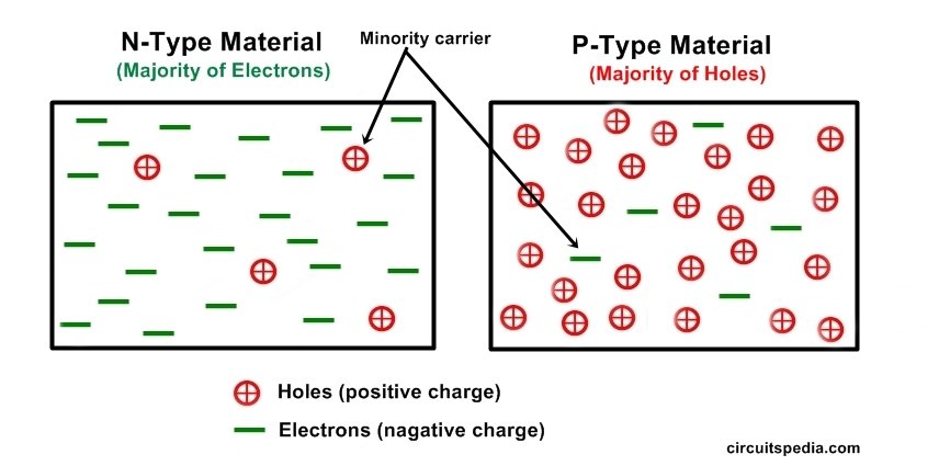
PN junction is made from a single piece of semiconductor of two different properties . One side is made to be P-type material and the other side is made with N-type. Both ends of the PN-junction have different properties. One end has an excess/majority of electrons and the other end has an excess/majority of holes.
The p-type semiconductor is formed by adding trivalent impurities in pure or intrinsic semiconductor and n-type semiconductor is formed by adding pentavalent impurities in pure or intrinsic semiconductor.
P-type materials have majority charge carriers of holes, and minority charge carriers of electrons. But in N-type materials have majority charge carriers of electrons and minority charge carriers of holes .
Half part of a Si crystal is doped with trivalent impurity and half with pentavalent impurity, we get P-N junction diode. The border where p-type and n-region meets called the junction .
The free electrons move from negative terminal (cathode) to the positive terminal (anode) . But the current flow direction is from positive terminal to the negative terminal.
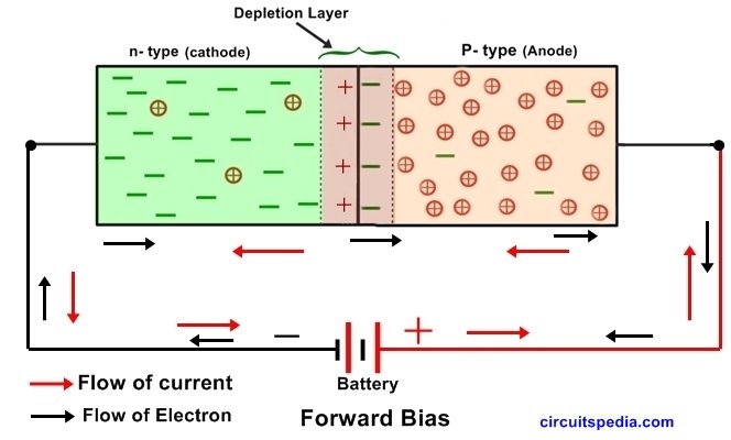
Forward bias- If p-terminal of diode is connected with positive supply and n-terminal is connected with negative supply then it is called forward bias. If the diode is forward biased, it allows the electric current flow. On the other hand, if the diode is reverse biased, it blocks the electric current flow.
Reverse bias- When p- terminal of diode is connected with n-terminal of supply and n- terminal is connected with p, this connection is called Reverse bias connection. In this connection no Electrons flow and no current flows.
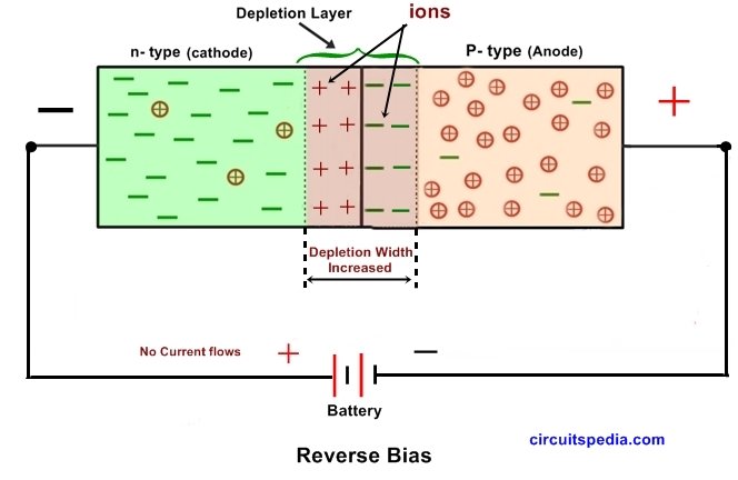
• Depletion layer-
Depletion layer created by the initial movement of majority carrier across the junction. Holes concentration on p- type and electron concentration on n-type are very high . Due to formation of p-n junction by diffusion electron moves from n-type to p-type and holes move from p-type to n-type. By the combination of electrons and holes at the junction creates ions, and there are presents only ions at the junction . Ions are non- movable.
Therefore when holes passes to electrons through these ions, then +ve ions repels the holes and oppose it passing to electron, And created a resistance wall of very small width . This is called Depletion layer. Width of depletion increases in reverse bias connection. An electric field intensity is created with depletion layer. and the sign of this electric field is negative because the direction of electric fields is +ve to -ve.
• Depletion layer consists +ve charge and –ve charge on either sides of junction.
• Depletion layer opposes only the the majority carrier not minority carrier.
• Depletion layer is also called Space charge region or transition region.
• Depletion layer consists immobile charge particles.
V-I Characteristics of Semiconductor P-N diode
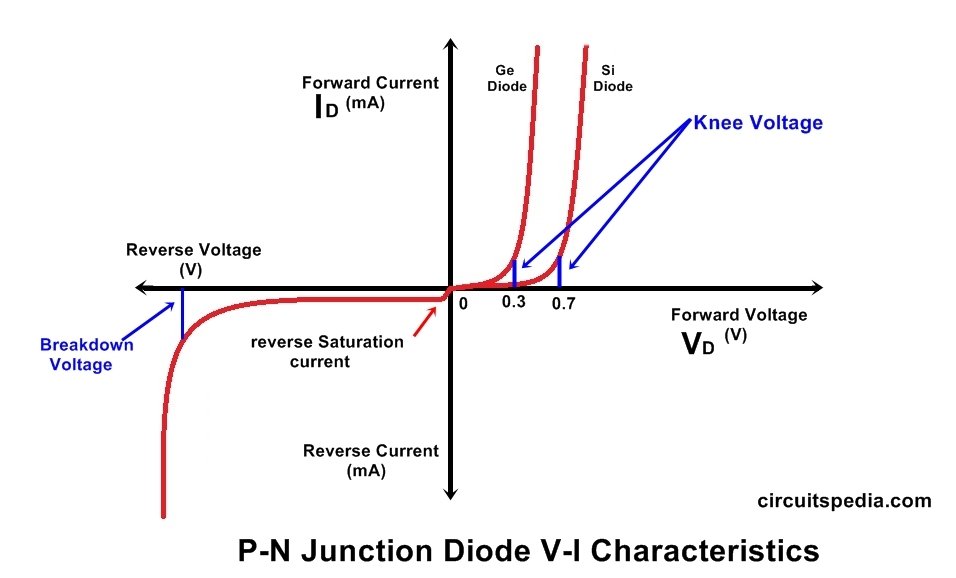
• Knee voltage-
This is the minimum required voltage to start the conduction of current through diode. This is also known as cut-in voltage. This is the forward voltage at which the diode current starts increasing rapidly.
The knee voltage of si diode is 0.7 voltage and 0.3v of Ge diode.
• Breakdown voltage-
This is the minimum amount of voltage of any insulator that makes it electrically conductor.
In Reverse bias connection of pn diode. no any current flows through diode, but when we increase the reverse voltage level continuously Then diode get internally damage (breakdown) and start conduction at a fix level. Breakdown voltage is the minimum Amount of reverse bias voltage at which diode starts conduction in reverse bias connection. This breakdown characteristics of diode uses in Zener Diode which is always used in reverse bias and Limits the circuit voltage.
• Doping-
A material in pure form acts like insulator. So making it more conductive in nature we need to add some impurity to it. The process of adding impurities in pure (intrinsic material) is called doping to change their electrical properties.Generally trivalent and pentavalent elements are used to doping to semiconductor .When a semiconductor is doped with trivalent impurity(Boron,Aluminium) ,it becomes P-type semiconductor material. When dope any intrinsic material with Pentavalent impurity (phosphorus, arsenic,bismuth,antimony) then it becomes N-type semiconductor.
• Reverse Saturation Current
Both sides of p-n junction a very small amount of minority charge carrier present. P type minority charge carrier in n-type side and n-type minority charge carrier on p-type side.It also allows to flow a minority charge current. The current which is flowing by the minority carriers is called Reverse current.
When a voltage applied on junction then further external reverse voltage flows due to minority charge carriers and this increases external voltage does not increases reverse current. At a voltage level where current goes on a fix maximum level and after Only voltage increases and curren does not increases . This is called reverse saturation current.
Reverse saturation current remain constant with the increase of voltage, But when voltage will increase continuously then at a Level of voltage when junction will get breakdown and high reverse current will flow.
Reverse saturation current depends on temperature. If temperature of junction increases , the minority charge carriers also increases.
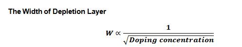
• The Width of Depletion Layer
Practically The value of Depletion width vary from 0.1µm to 0.5µm
Typical value of Depletion width is -0.5µm
By increasing doping concentration Depletion layer width can Reduced
electrons moves across the PN junction from the N-type to the P-type , they leave behind positively charged donor ions on the negative side. Holes from the acceptor impurity moves across the junction in the opposite direction into the region where there are large numbers of free electrons.
As a result, the charge density of the P-type through the junction is filled with negatively charged acceptor ions , and the charge density of the N-type along with the junction becomes positive. This charge transfer of electrons and holes across the PN junction is known as diffusion .
• Barrier potential/built in potential
Simply Voltage form across the depletion layer is called the contact potential. The built-in potential in a semiconductor equals the potential across the depletion region in thermal equilibrium.This is also called built-in potential or barrier voltage/potential or potential hill or diffusion voltage.
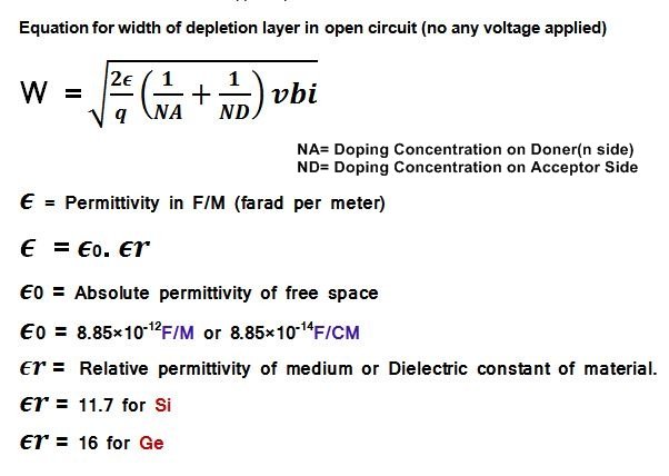
Contact potential always appear with in depletion layer It is noted as V0 or vbi.
Contact potential of any diode can not measure by any instrument.
V0 for Ge diode = 0.1v to 0.5v typically we use V0=0.2v
V0 for Si diode = 0.6v to 0.9v typically V0= 0.7v
Application of p-n junction diode
• As Rectifier to convert AC to DC signal
• Clipper circuit for clipping the signal (changing the wave shape)
• To supply ( for protection from reverse supply)
• Clamper circuit to restore the dc signal wave
• As Voltage multiplier
• In digital logic design
• In Demodulation Circuits
Other types of diode
Photodiode, Zener Diode, Gunn Diode, Tunnel Diode. PIN Diode, Varactor Diode. Light Emitting Diode (LED), Schottky Diode, Laser Diode, Switching Diode.
Also read
-
What is impedance (circuitspedia.com)
Impedance (Z) is similar to Resistance (R) . Impedance and Resistance both oppose the current in circuit. Both are almost the same thing , But resistance related to DC Circuit. Resistance oppose the steady electric current in DC circuit. Resistance remains same (constant) at any different frequency range.
Impedance is related with AC circuit. Impedance vary according to changing the frequency, this is not constant at different frequency range. Impedance also includes reactance (Inductive and capacitive property of the circuit).
Reactance - Reactance is the Resistance produced to AC Currents by Inductors and Capacitors only. This is a measure of the type of opposition to AC electricity due to capacitance or inductance.
The impedance is denoted by Z and unit of it is Ohm (Ω).
If the level of ohm is higher then level impedance is also higher.
Impedance = Resistance + Reactance (Either inductive or Capacitive or both)
In DC circuit, Impedance is effective Resistance of the circuit.
Z= R
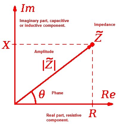
In AC circuits, it possesses both magnitude and phase, unlike resistance, which has only magnitude.
In the case of capacitor, When the frequency increased then the resistance (Impedance ) of capacitor decreases. In Inductor this is just opposite, When we increase the frequency range then Impedance increase in inductor.
Impedance
Impedance is defined as combination of resistance and reactance.

As we cannot assume any circuit with DC Current without Resistance , We cannot assume a circuit with AC current without Impedance.
Resistive Power- Energy burns by resistive power to Heat goes through that system ,
In Reactive Power- the energy goes to Antennas, Speaker, transmission line, cable etc represents how much energy to be stored and propagates. Not burn to heat ie Impedance.
Resistance
If there is Only Resistor is connected with Load in any circuit then is called Resistor.

• Reactance
If any circuit there is Only inductor or capacitor connected with load. Then the value of v/I is called reactance.
In Reactance There are 2 cases
(1) If inductor in connected then in this case reactance is called inductive reactance,

and its value in scalar form XL = ѡL, and in vector form XL=JѡL Where ѡ=2Πf. Here If frequency is increased then the value of wL is also increased.
(2) If Capacitor is connected then the Reactance is called Capacitive Reactance and it is denoted by (scalar form) Xc =

In vector form
Where
If frequency (f) is increased then value of Xc is decreased. ie ω inversly proportional to 2Πf.
♦ Impedance – If Any circuit consist Resistance -Inductor. Or Resistance - Capacitor, Or Resistance-inductor-Capacitor. Then the value of v/I is called Impedance.
It is denoted by
-
If Resistor(R) and Inductor(L) connected –The value of Impedance (scaler form)

In vector form Z= R+jωL
- If Resistor (R) and Capacitor(C) connected - Then
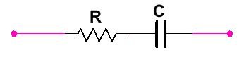
Impedance
And In vector form impedance
- If Resistor (R) , Inductor (L) capacitor (C) Connected - Then
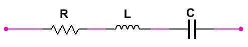
Impedance
In vector form
Phasor Diagram of Impedance
Unit
- Impedance - Ω
- Reactance - Ω
- Resistance - Ω
Download
also read
-
If Resistor(R) and Inductor(L) connected –The value of Impedance (scaler form)
-
LOGIC GATES
Logic gates are the basic building elements of any digital systems or circuits. The name Logic gate is derived from the sense of the making decisions ability of such a device, and after making decisions it produce one output result. We can say that Logic gates are the fundamental building blocks of any digital circuits or digital systems.
There are 3 basic Types of Logic gates – (1)-AND , (2)-OR , (3)-NOT
Basically Logic gates are elementary electronic logic circuit that can make a variety of different types of circuits by interconnection of these three gates to perform complex logically operations of any computer. This is called logic design. Logic gates made a number of electronic devices and other digital components. In practical application of logic gates we see in the form of different Ics. These Ics are in LSI (Large scale integration), VLSI (Very large scale integration ) and SSI (Small scale integration) . Input and Outputs of Logic gates in only two levels called TRUE and FALSE , or HIGH and LOW, or ON and OFF, or very popular 0 and 1.
High (1 or TRUE or ON) means +5v
LOW(0 or FALSE or OFF) means 0v (or -ve supply)
These 2 level logic also called Positive and Negative Logic.
AND GATE
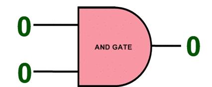
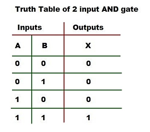
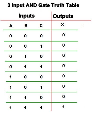
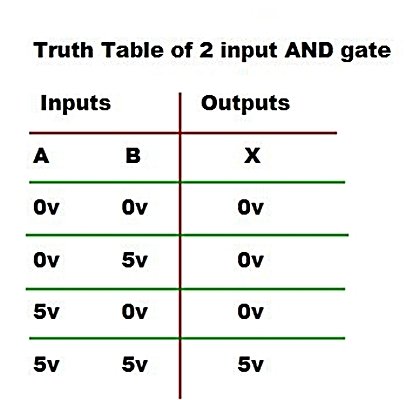
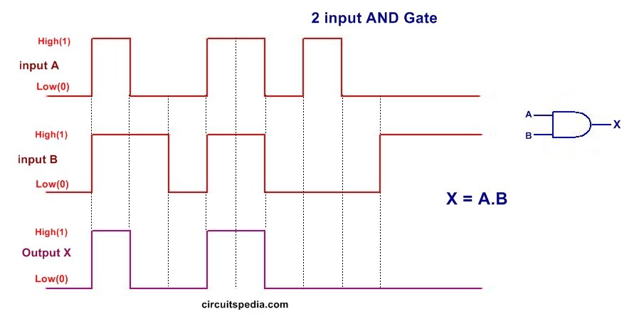
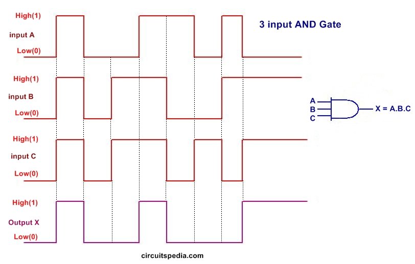
AND gate has two or more than two inputs and only one Output. In AND gate Output is High or 1 only when each input of it has in HIGH state. Means output is 1 if only all inputs are at 1 level. If any one input goes at 0 level then the output of AND gate becomes 0 .
Logic Symbol
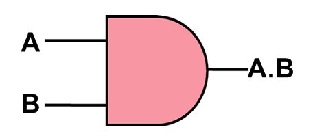
Input Variables are represented by A,B,C…… and the the output is written as X. In the Boolean expression it can be written as X=A.B.C……. It Can be read as X is equal to A and B and C ….or X is equal to A dot B dot C…. or X is equal to ABC…..
Realization of AND Gate-
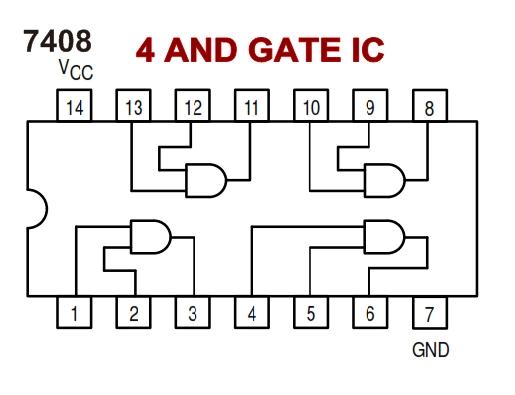
AND gate may be realized by the using of diode and transistors. If it made by using diodes then it called as DL(Diode Logic) and if using transistors it called as RTL (Resistor Transistor Logic) .
In the Diode Logic AND gate When the input A = +5v and input B is also +5v, in this case both diodes D1 and D2 are off (because of reverse mode). And therefore no current flows through resistor R. So no voltage drop occurs across R and voltage remain at the output is HIGH.
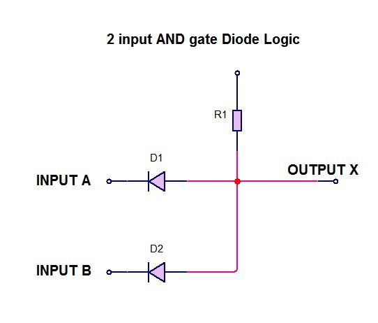
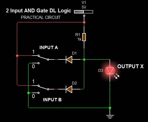
When A=0, and B=0v or any one of A or B is 0v. Then the both diodes or corresponding Diode D1 or D2 are ON and the circuit is act as short circuit. In this condition the output X=LOW or 0v.
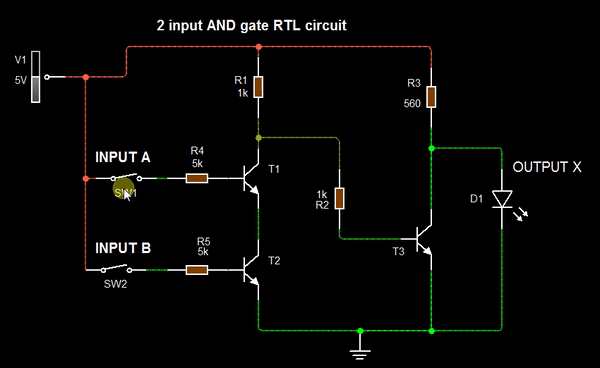
RTL AND Gate circuit
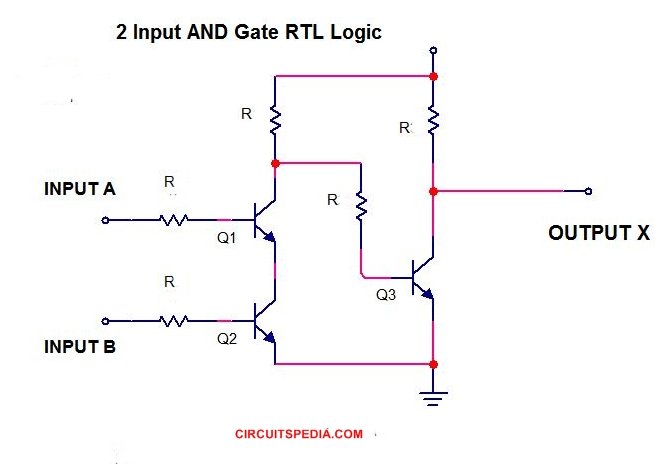
In the RTL AND gate or transistor gate, When A=0v and B=0v. Then the transistors Q1 and Q2 are off but transistor Q3 remain in ON, and the voltage at output is LOW or 0v because of Q3 ON and current pass through Q3 and voltage is dropped through R.
If Any one of input A or B is high then Either Q1 or Either Q2 will off and then no voltage drop occurs at R. So Q3 Will remain in turn on and therefore output will LOW.
If input A and input B both are HIGH then both transistors Q1 and Q2 will turn on and current passes through these transistors between ground and +5v and voltage will LOW at the collector pin of T1 and at input of Q3 . So Q3 will off and no voltage drop at collector pin and output will HIGH. At HIGH condition the voltage at output is approx 5v (X≈5v).
Also read Ultrasonic Distance measurement project using Arduino
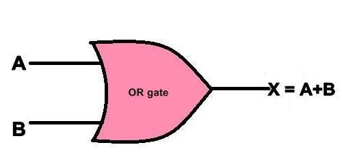
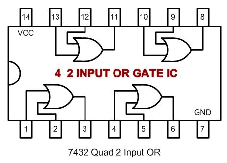
OR gate-
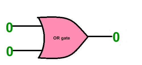
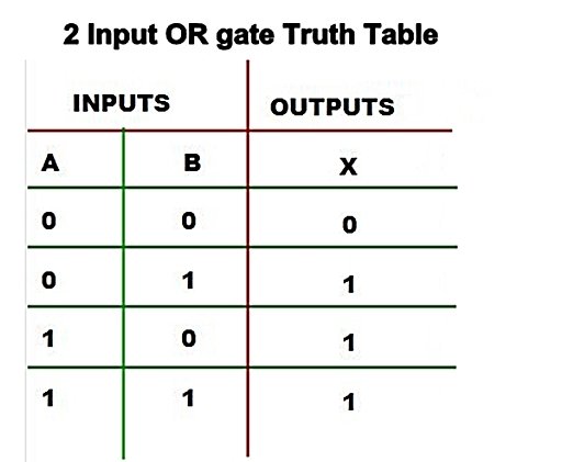
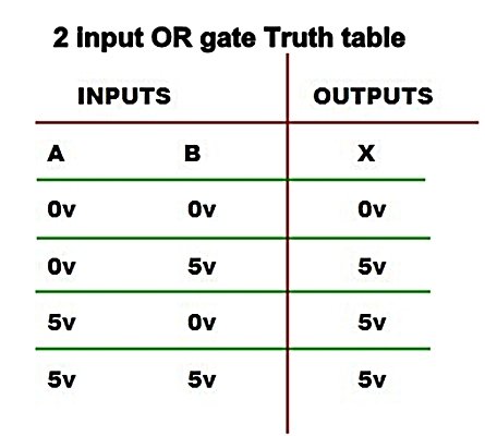
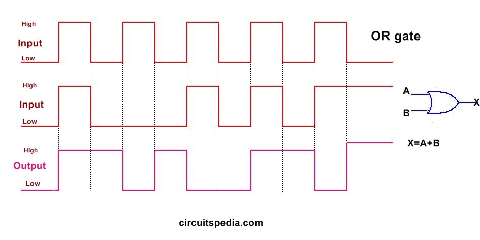
OR gate have also two or more than two inputs but only one output. The output is HIGH or 1 if even any one of input is 1. The output is o or LOW if all of its input is in LOW state or 0 . OR gate is defined as the device which output is o if any one of its input is 1.
Must read What is NOT gate
The Logic symbol for OR gate is +. The Boolean expression for the output can be written as X=A+B+C+…… This is written as X is equal to A plus B plus C or it can also be read as X is equal to A or B or C or ….. .
Realization of OR gates can be made using Diodes(Diode Logic) or Transistors(RTL).
In the diode or gate, when both input A and B=0v or LOW , then both diodes D1 And D2 are OFF state because of reverse biasing. So No any current pass Through R and No voltage drop will occur . Then the output X=0v . If both input or any one of both input are +5v . Then the corresponding diode D1 or D2 is On or both diode D1 and D2 are ON and short circuit occur across them. Therefore the output X is approx to +5v. voltage drop across diode is +5v-0.7v= 4.3v . But this is treated as HIGH or 1.
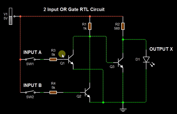
In the Transistor (RTL) logic OR gate circuit, When both input A & B are 0v. Transistors Q1 and Q2 are OFF and Transistor Q3 is ON because of it get Base voltage through Resistor R1. So the output voltage at Collector pin of Q3 go 0v by dropping of voltage with ground at R2 . If any one of any input A or B is HIGH or 1 then the corresponding transistors in ON state . So voltage at the collector of that transistor goes to 0v by voltage drop and there is no any Base voltage at the Q3 and no any voltage drop occurs at R2 therefor the output is HIGH OR 1.
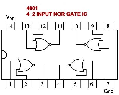
The Universal Gates
Universal gates are defined as Which logic gates can implement any types logic gates . There are two universal gates NAND and NOR. Both NAND and NOR gates can perform all the three basic logic functions of AND, OR, NOT. AOI (AND/OR/INVERT(NOT)) can be converted to NAND logic or NOR logic.
Types of Universal Gates
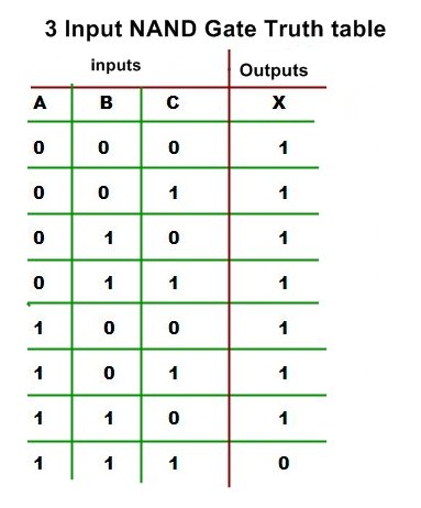
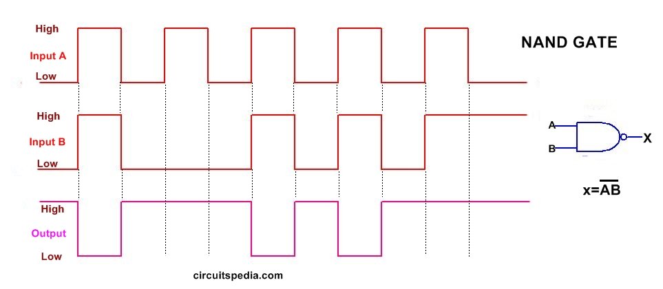
NAND Gate (NOT-AND)
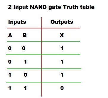
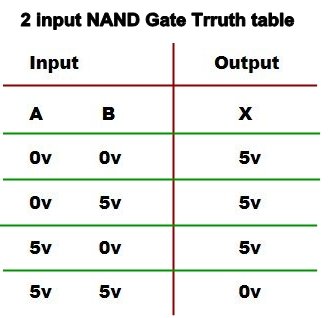
NAND gate is a combination of AND gate and NOT gate. If the output of AND gate is Inverted then it is called NAND gate. NAND = NOT AND. When AND output is NOTed or Inverted then it is called NAND gate.
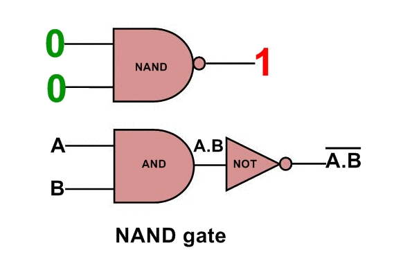
The output is 0 only if each inputs is 1 and output is 0 if any one of any input or all inputs are 0. Means when all inputs are 1 then output will 1 otherwise if different combination of input the output is 0. The boolean expression of NAND gate is written as X=

This is read as X=A.B.C….whole bar.
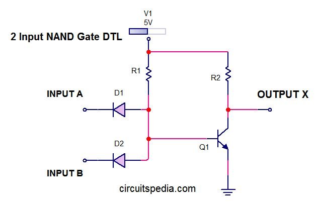
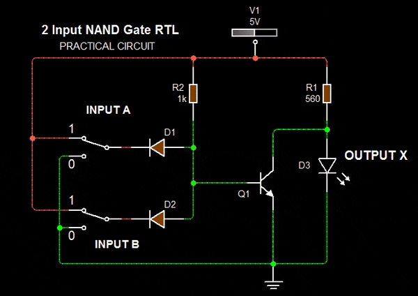
Realization of NAND gate -
A two input NAND gate can be realized using Diode Transistor Logic. When the input A and B both are HIGH or +5v then both diodes are off and transistor get base voltage through R1 . So the transistor is ON and the output voltage at collector is 0v because of dropped voltage with ground. When Both input A and B are 0v then the both diode are in ON because of forward bias (here 0v means negative supply) . So Base voltage of transistor is 0v. So Transistor is in OFF and then the output is HIGH or approx +5v.
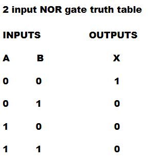
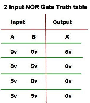
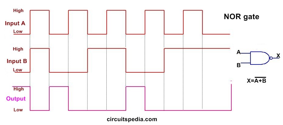
NOR Gate
When the output of OR gate is NOTed or inverted then it is called NOR gate. NOR means NOT OR. NOR gate is the combination of an OR gate and a NOT gate. The output is 1 or HIGH when only the both input is 0 or LOW. Otherwise output is 0. The boolean expression for the NOR gate is expressed as given below This is read as X is equal to A plus B plus C plus .....whole bar.
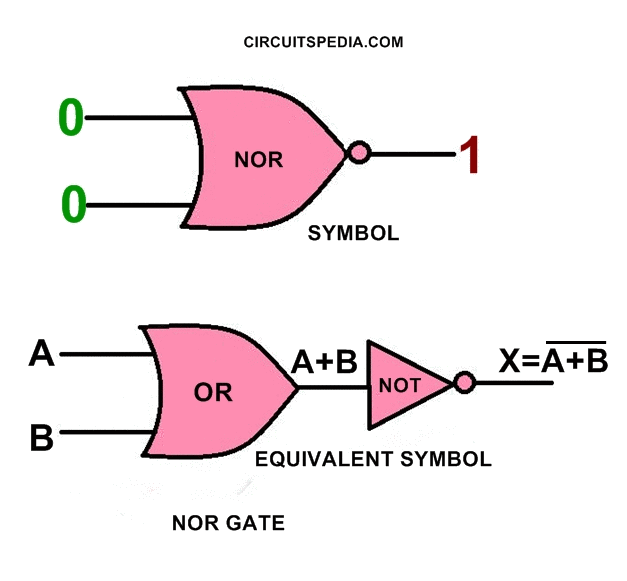
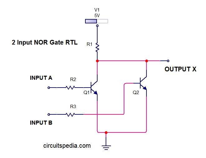
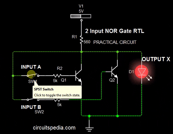
Realization of NOR gate-
For more circuits and tutorials click here
Two input RTL(Resistor transistor logic) NOT gate can be realized using two transistors and resistors. When Input A and B both are 0. A=0 and B=0. Then both transistors are OFF because no base voltage get. So no current flows through transistors and no voltage drop occurs. Therefore only current passes through R the output is HIGH.
Also read Arduino remote control AC load
-
LOGIC GATES
Logic gates are the basic building elements of any digital systems or circuits. The name Logic gate is derived from the sense of the making decisions ability of such a device, and after making decisions it produce one output result. We can say that Logic gates are the fundamental building blocks of any digital circuits or digital systems.
There are 3 basic Types of Logic gates – (1)-AND , (2)-OR , (3)-NOT
Basically Logic gates are elementary electronic logic circuit that can make a variety of different types of circuits by interconnection of these three gates to perform complex logically operations of any computer. This is called logic design. Logic gates made a number of electronic devices and other digital components. In practical application of logic gates we see in the form of different Ics. These Ics are in LSI (Large scale integration), VLSI (Very large scale integration ) and SSI (Small scale integration) . Input and Outputs of Logic gates in only two levels called TRUE and FALSE , or HIGH and LOW, or ON and OFF, or very popular 0 and 1.
High (1 or TRUE or ON) means +5v
LOW(0 or FALSE or OFF) means 0v (or -ve supply)
These 2 level logic also called Positive and Negative Logic.
AND GATE
AND gate has two or more than two inputs and only one Output. In AND gate Output is High or 1 only when each input of it has in HIGH state. Means output is 1 if only all inputs are at 1 level. If any one input goes at 0 level then the output of AND gate becomes 0 .
Logic Symbol
Input Variables are represented by A,B,C…… and the the output is written as X. In the Boolean expression it can be written as X=A.B.C……. It Can be read as X is equal to A and B and C ….or X is equal to A dot B dot C…. or X is equal to ABC…..
Realization of AND Gate-
AND gate may be realized by the using of diode and transistors. If it made by using diodes then it called as DL(Diode Logic) and if using transistors it called as RTL (Resistor Transistor Logic) .
In the Diode Logic AND gate When the input A = +5v and input B is also +5v, in this case both diodes D1 and D2 are off (because of reverse mode). And therefore no current flows through resistor R. So no voltage drop occurs across R and voltage remain at the output is HIGH.
When A=0, and B=0v or any one of A or B is 0v. Then the both diodes or corresponding Diode D1 or D2 are ON and the circuit is act as short circuit. In this condition the output X=LOW or 0v.
RTL AND Gate circuit
In the RTL AND gate or transistor gate, When A=0v and B=0v. Then the transistors Q1 and Q2 are off but transistor Q3 remain in ON, and the voltage at output is LOW or 0v because of Q3 ON and current pass through Q3 and voltage is dropped through R.
If Any one of input A or B is high then Either Q1 or Either Q2 will off and then no voltage drop occurs at R. So Q3 Will remain in turn on and therefore output will LOW.
If input A and input B both are HIGH then both transistors Q1 and Q2 will turn on and current passes through these transistors between ground and +5v and voltage will LOW at the collector pin of T1 and at input of Q3 . So Q3 will off and no voltage drop at collector pin and output will HIGH. At HIGH condition the voltage at output is approx 5v (X≈5v).
Also read Ultrasonic Distance measurement project using Arduino
OR gate-
OR gate have also two or more than two inputs but only one output. The output is HIGH or 1 if even any one of input is 1. The output is o or LOW if all of its input is in LOW state or 0 . OR gate is defined as the device which output is o if any one of its input is 1.
Must read What is NOT gate
The Logic symbol for OR gate is +. The Boolean expression for the output can be written as X=A+B+C+…… This is written as X is equal to A plus B plus C or it can also be read as X is equal to A or B or C or ….. .
Realization of OR gates can be made using Diodes(Diode Logic) or Transistors(RTL).
In the diode or gate, when both input A and B=0v or LOW , then both diodes D1 And D2 are OFF state because of reverse biasing. So No any current pass Through R and No voltage drop will occur . Then the output X=0v . If both input or any one of both input are +5v . Then the corresponding diode D1 or D2 is On or both diode D1 and D2 are ON and short circuit occur across them. Therefore the output X is approx to +5v. voltage drop across diode is +5v-0.7v= 4.3v . But this is treated as HIGH or 1.
In the Transistor (RTL) logic OR gate circuit, When both input A & B are 0v. Transistors Q1 and Q2 are OFF and Transistor Q3 is ON because of it get Base voltage through Resistor R1. So the output voltage at Collector pin of Q3 go 0v by dropping of voltage with ground at R2 . If any one of any input A or B is HIGH or 1 then the corresponding transistors in ON state . So voltage at the collector of that transistor goes to 0v by voltage drop and there is no any Base voltage at the Q3 and no any voltage drop occurs at R2 therefor the output is HIGH OR 1.
The Universal Gates
Universal gates are defined as Which logic gates can implement any types logic gates . There are two universal gates NAND and NOR. Both NAND and NOR gates can perform all the three basic logic functions of AND, OR, NOT. AOI (AND/OR/INVERT(NOT)) can be converted to NAND logic or NOR logic.
Types of Universal Gates
NAND Gate (NOT-AND)
NAND gate is a combination of AND gate and NOT gate. If the output of AND gate is Inverted then it is called NAND gate. NAND = NOT AND. When AND output is NOTed or Inverted then it is called NAND gate.
The output is 0 only if each inputs is 1 and output is 0 if any one of any input or all inputs are 0. Means when all inputs are 1 then output will 1 otherwise if different combination of input the output is 0. The boolean expression of NAND gate is written as X=
This is read as X=A.B.C….whole bar.
Realization of NAND gate-
A two input NAND gate can be realized using Diode Transistor Logic. When the input A and B both are HIGH or +5v then both diodes are off and transistor get base voltage through R1 . So the transistor is ON and the output voltage at collector is 0v because of dropped voltage with ground. When Both input A and B are 0v then the both diode are in ON because of forward bias (here 0v means negative supply) . So Base voltage of transistor is 0v. So Transistor is in OFF and then the output is HIGH or approx +5v.
NOR Gate
When the output of OR gate is NOTed or inverted then it is called NOR gate. NOR means NOT OR. NOR gate is the combination of an OR gate and a NOT gate. The output is 1 or HIGH when only the both input is 0 or LOW. Otherwise output is 0. The boolean expression for the NOR gate is expressed as given below This is read as X is equal to A plus B plus C plus .....whole bar.
Realization of NOR gate-
For more circuits and tutorials click here
Two input RTL(Resistor transistor logic) NOT gate can be realized using two transistors and resistors. When Input A and B both are 0. A=0 and B=0. Then both transistors are OFF because no base voltage get. So no current flows through transistors and no voltage drop occurs. Therefore only current passes through R the output is HIGH.
Also read Arduino remote control AC load
-
In this project, a complete design and development procedure of a digital thermometer has been discussed. The algorithm used in this design is simple and easy to understand. The components used are limited and readily available in the market. Although the overall development of this project is lowcost and easy still the results are extraordinary. Let’s see how this design works.
Arduino and LM35 based digital thermometers can be developed at home with very few components and instruments needed. Arduino UNO used in this design is a microcontroller which is responsible for data handling and processing for temperature calculation and display. Arduino UNO has digital I/O and Analog pins. In this case, we are using both.
The next component is LM35 which is a temperature sensor and looks more like a simple BJT. LM35 is cheap as compared to most of the temperature sensors and yet offers a high level of accuracy even at extreme temperatures. LM35 can be used in both analog circuits and embedded systems since it offers analog voltages at the output.
The circuit diagram described in this simulation video is simple and can be easily modified if needed. Click For Full Project Detail
Simulation Video
Testing VideoClick for Coding and full project detail
.
-
-----------------------------------------------------
This Inverter circuit is given from a trusted youtube channel on the robotics. He is showing in video on breadboard using this circuit.
As name this is a simple inverter, so how this can powerful and regulated ???? Output Power is Also Depend on Transformer Ampere.
In text also advised to use minimum of 1 A Transformer, not only 1 A
Your corrected circuit is correct but my circuit is not wrong. One BD140 PNP transistor was also connected as here on that video.
-
12 hours ago, audioguru said:
This is not wrong . This is right
-
100% working
This diagram was given by one user that used already this circuit at home by implement from This diagram.
No Direct supply given on ic. capacitor may only one issue
Which inverter circuit is wrong , please tell me , I will checked and modifiy
This diagram is given by one user that used already this project at home by implement from This diagram.
Which inverter circuit is wrong , please tell me , I will check and modify
-
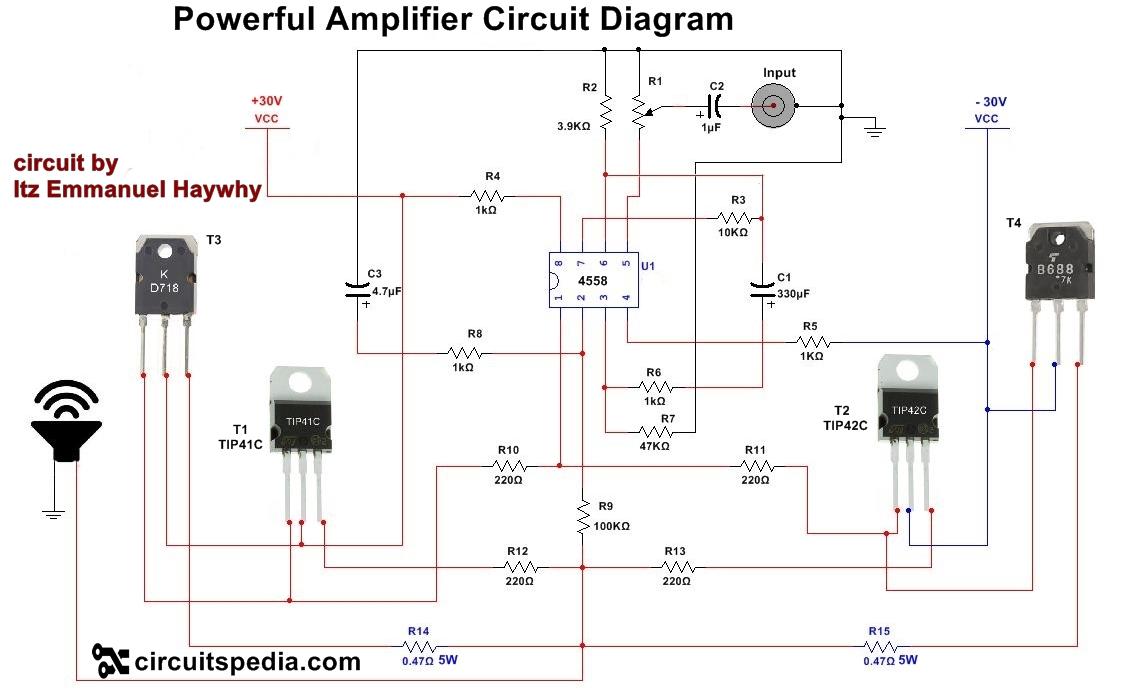
4558 ic Audio Power Amplifier Circuit Diagram
This is circuit diagram of powerful audio amplifier. This circuit is given by Emmanuel. In this circuit one ic 4558 and 4 Power transistors are used with some discrete components. Use 20v-to 60v for operating this circuit. This is a single channel audio amplifier circuit. Use capacitor of minimum 50v value. Positive supply voltage is given at the middle pin of both transistor TIP41C and D718. Negative supply is given at middle terminal of D688and TI42C Transistor. R1 is the variable resistor potentiometer for volume control. This vol. control may be value of 50k to 100k. Use Big size speaker with this circuit. 4558 Audio Amplifier Circuit Diagram.
In image of assembled kit there is no 5w resistor connected
 for more Amplifier circuit click here

-
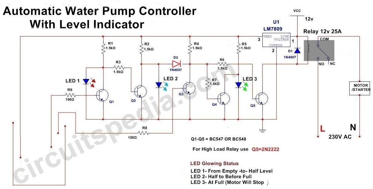
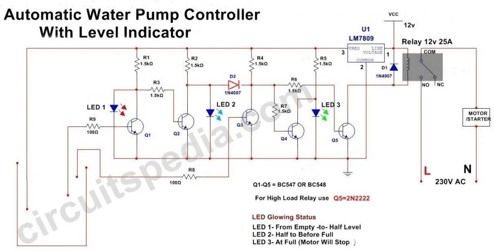 This is an Automatic submersible Motor controller circuit using transistor
• The Main Advantage Of this Project Is To All Three LEDs Are Glowing One by One. Only One LED is Glowing At One Level And Other Two Are in Off state.
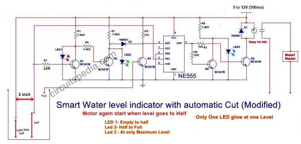
Below is a modified ckt that has advantage of Motor will Again start only if the water level goes to less than half
For more circuits go to www.circuitspedia.com
-
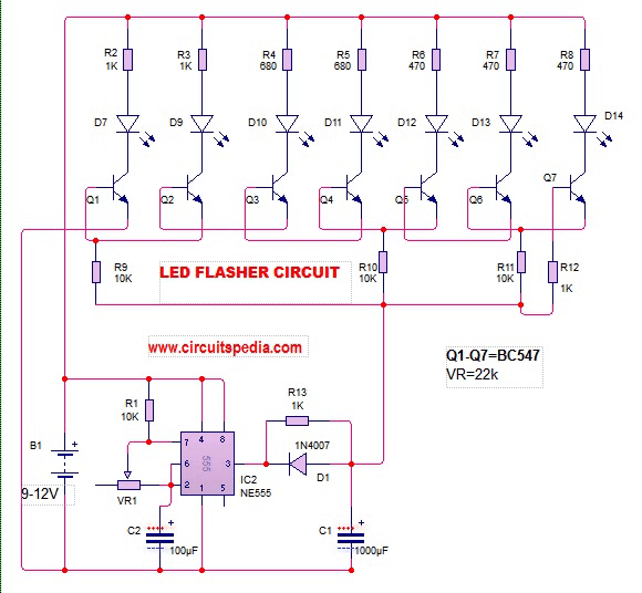
http://www.circuitspedia.com/blinking-led-flasher-circuit-diagram-with-555/
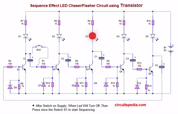
http://www.circuitspedia.com/simple-5-led-blinker-flasher-circuit-blinking-led-running-chaser-light/
17 LED Sequencer/Flasher Circuit using 2 Counter ic 4017
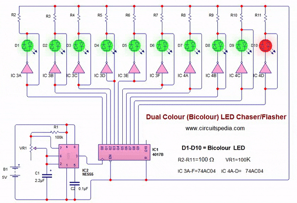 Dual colour led flasher circuit
For more circuit go to circuitspedia.com
-
The LM3914 is a monolithic integrated circuit that senses analog voltage levels and drives 10 LEDs, providing a linear analog display. This ic is used for Dot and Bar Display. A single pin changes the display from a moving dot to a bar graph. Current drive to the LEDs is regulated and programmable, eliminating the need for resistors. This feature is one that allows operation of the whole system from less than 3V.
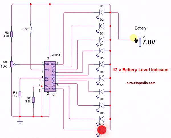
From datasheet – The linear scaling of the output thresholds makes the device usable, for example, as a voltmeter. In the basic configuration it provides a ten step scale which is expandable to over 100 segments with other LM3914 ICs in series.
The simplified LM3914 block diagram is to give the general idea of the circuit’s operation. A high input
impedance buffer operates with signals from ground to 12V, and is protected against reverse and overvoltage
signals. The signal is then applied to a series of 10 comparators; each of which is biased to a different
comparison level by the resistor string.For more detail Click Here
.
-
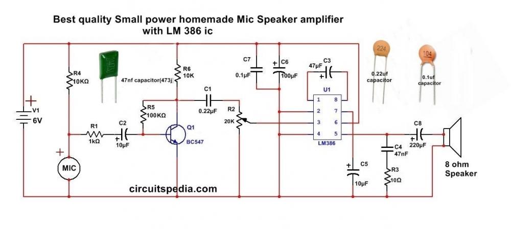
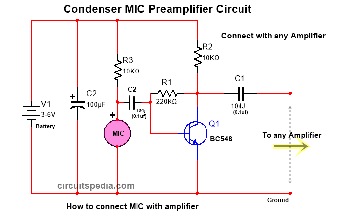
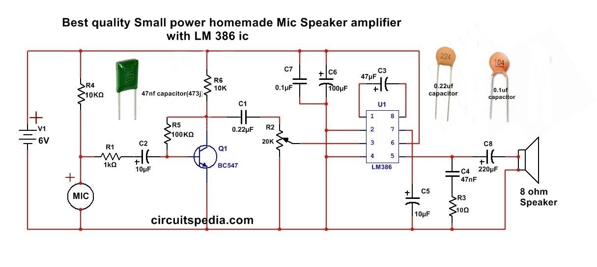
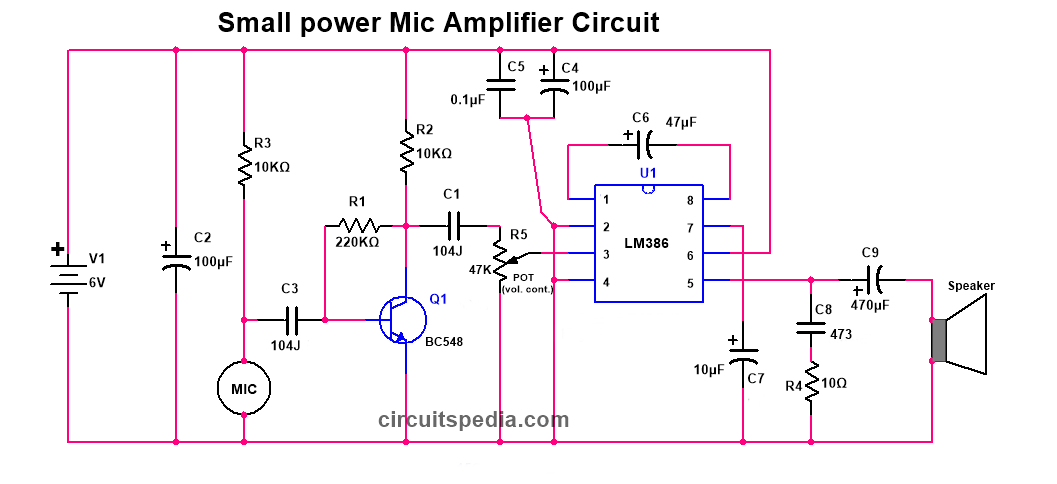
Homemade MIC Amplifier Loudspeaker connection circuit
You can connect condenser MIC with any amplifier circuit as given below diagram . This circuit will work very well with any type of Audio amplifier. Use only 3-5v for condenser MIC for best result. Audio amplifier circuit need 6-24v as per amplifier specification.
Connect the positive terminal of mic with 22k resistor in series with positive supply and negative terminal of mic is directly connected to negative supply or ground. And enjoy this easy homemade MIC Loudspeaker.
This Circuit works with any type of amplifier circuit.
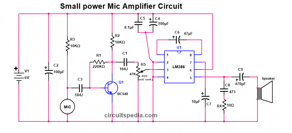
If you have no any audio amplifier then you can make an small amplifier very easily with LM386 ic. This is very popular amplifier ic and available on any electronic part store.
You can check for more simple circuit here circuitspedia.com
-
-
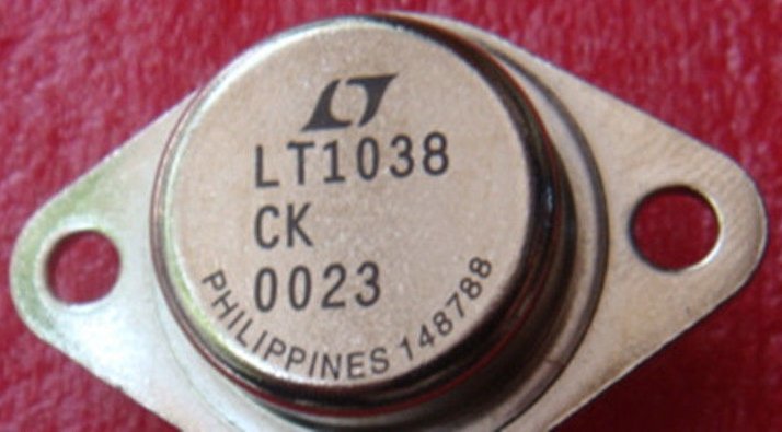
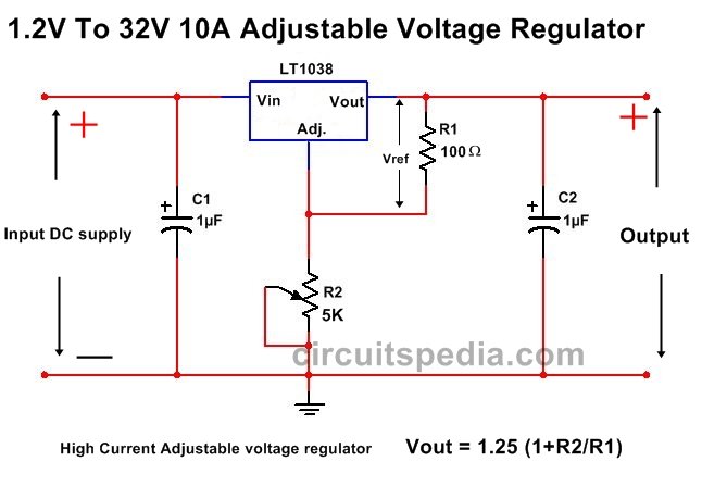
10A High Current Adjustable Voltage Regulator using LT1038
-
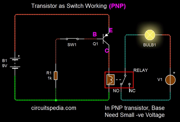
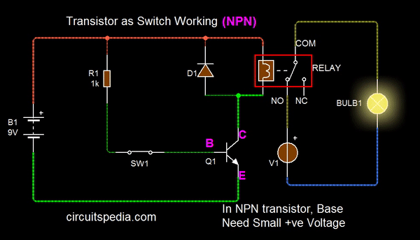
http://www.circuitspedia.com/transistor-as-switch-working-how-transistor-works/
A small Positive current required at the Base terminal for the turning on the transistor. By sending varying levels of current to the base, the amount of current flowing through the collector to emitter may be regulated.
When we apply a small Positive supply at base , then Current between emitter and collector will passed and we say that transistor is turn on. A very small amount of current may be used to control a large amount of current, this property is known as amplifier . .
A Diode with Parallel of relay coil in reverse connection is necessary for protection the transsistor. This must connected on both PNP and NPN


Siren Sound | Bird Sound | Tone generator using 555 timer
in Electronic Projects Design/Ideas
Posted
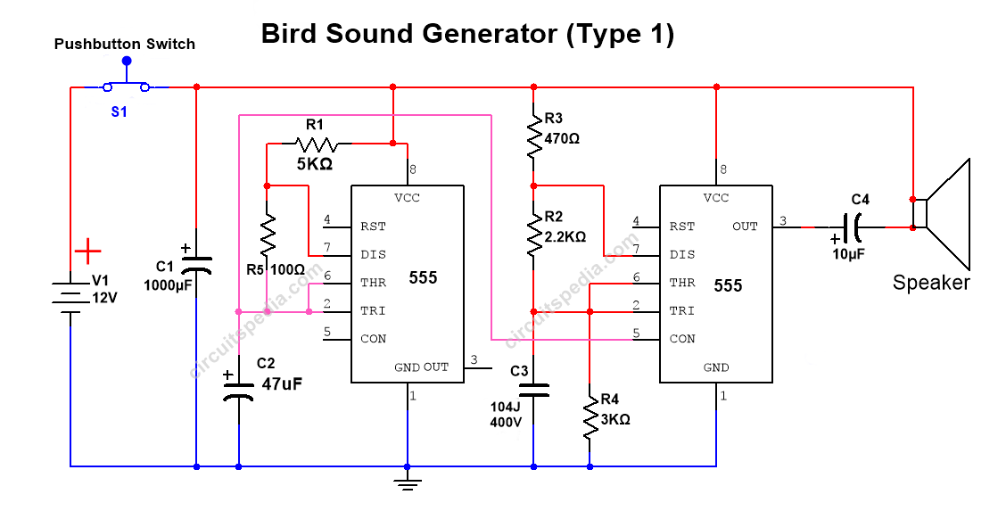
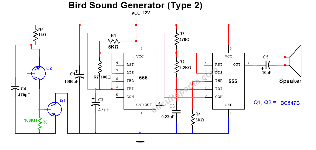
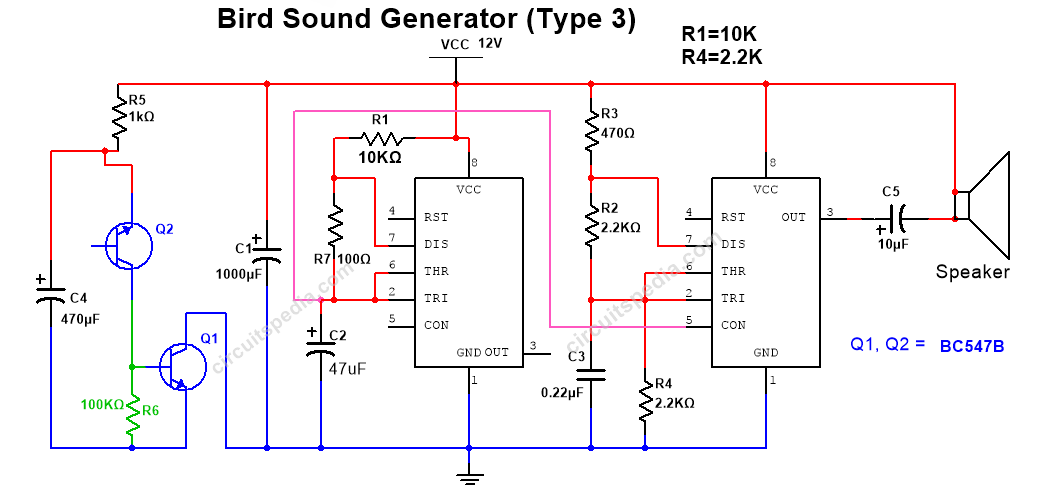
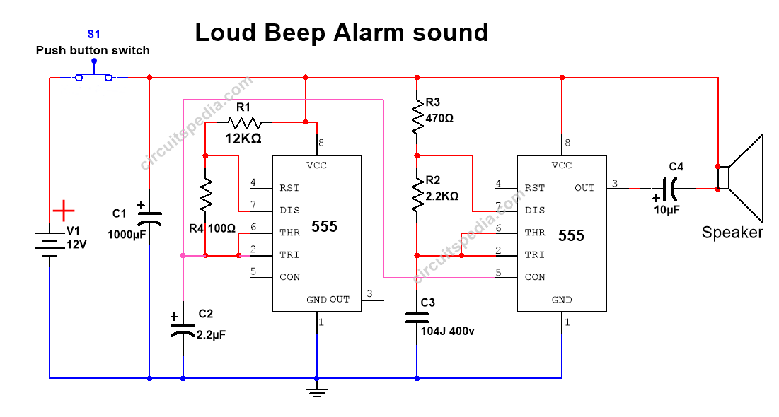
Tone generator circuit using 555 timer
Bird sound generator, Ambulance Siren Generator
These are some circuit diagrams of the sound generators. Sounds are like Bird sound, Ambulance siren, Beep Horn, and other different types. Use 9 to 12v Dc supply and components value should be the same as suggested in the diagram because any variation of components value can change the sound type.
By some changes of values of some components as given below in the diagram, you can produce many different types of sounds. Use a medium-size speaker, These circuits can be useful for the making of an Alarm, Doorbell or other warning indicators.
schematic diagram
Bird sound generator circuit
http://circuitspedia.com/wp-content/uploads/2020/09/bird-sound-generator-circuit-using-555.png
http://circuitspedia.com/wp-content/uploads/2020/09/bird-sound-generator-circuit-diagram-using-555-timer-1.png
http://circuitspedia.com/wp-content/uploads/2020/09/bird-sound-generator-circuit-diagram-555-timer.png
Alarm sound generator circuit diagram
http://circuitspedia.com/wp-content/uploads/2020/09/horn-sound-generator-circuit-using-555-timer.png
http://circuitspedia.com/wp-content/uploads/2020/09/siren-sound-generator-circuit.png
http://circuitspedia.com/wp-content/uploads/2020/09/beep-sound-circuit-1.png
Ambulance sound generator circuit diagram
http://circuitspedia.com/wp-content/uploads/2020/09/555-timer-siren-sound-generator-circuit.png
Testing Video
What is Opto-coupler/opto-Isolator
Arduino Remote control AC Dimmer
Switch ON Delay Timer circuit
High power inverter with charger circuit diagram
Infrared proximity sensor circuit
Dark sensor circuit - 4 circuit