

AN920
-
Posts
359 -
Joined
-
Last visited
Never
Content Type
Profiles
Forums
Events
Posts posted by AN920
-
-
Changing the value of the resistor will vary the frequency. This type of oscillator works because of a negative resistance region created at the reverse breakdown potential level. You should not make the resistor too low and damage the transistor.
I have done some experiments on this type of circuit and found that the upper limit of oscillation to be around 200kHz. I used it as a VCO by varying the applied voltage between 8-30V. It gave quite a good saw tooth wave with constant amplitude of 3Vp-p
I even managed to get it oscillating with a low frequency crystal (32kHz) but it is a bit tricky to get going. The output is then a nice sine wave. -
Typical Ku factors for standard converters:
Forward 0.4
Full and 1/2 bridge 0.4
Push Pull w CT 0.4 ~ 0.5 (0.5 for the single ended secondary output)
This sounds low but due to the shape of standard round copper wire, if you do the math only about 78% of the available window area can be filled. Take the insulation of the wire, any other layer insulation, mandatory creepage distances, RFI and safety screens. Add the bobbin and you can start to see the picture.
Construction with foil windings will also improve Ku
Planer designs may have slightly higher factors. -
This shows the potential problem(1) of the circuit. In normal operation with a low load impedance there would be no problems. It is always good to be aware of such problems when used in certain applications.
Example: If the output is sensed by another very high impedance instrument like in automated test setup, problems may show.
First condition show that even though the transistor should be off, there is a leakage current of 170pA flowing in the b-e junction. This causes 74nA to flow in the collector, which will read as 7.47V on our measuring instrument. That error could halt out test process as detecting a fault.
This must be caused by leakage from U1's (off-state open collector impedance) and D1's reverse leakage current. Note that this leakage current will roughly double with each 10deg C increase in temperature. We must also be aware that the leakage of D1 will be aggravated by light shining through the glass body on the internal junction. Shield it from light.
To see the contribution by each, we open U1(pin1) and see that we still have 123pA through D1. Voltage on Q2 collector is still 6.09V
By adding a resistor (10k in this example, but anything up to 100k will do), we cancel or reverse this current flowing out of Q2 base. This is now -58pA, and our measuring instrument measures only 5.96mV on Q2 collector. Note the collector leakage current of Q2 is now about 1000 times smaller. -
The circuits won't work with a normal opamp and is meant to use a open collector comparator.
The following diagrams show one of the problems I stated earlier
The first two diagrams show the circuit in both conditions. ( I only left the switches in their respective states for clarity). It can be seen from the simulation that LED1 is always on, while LED2 is off in the SET state.
Next is the circuit that uses another PNP transistor driven from the collector of first PNP. Simulation voltages show the results.
You need to zoom in otherwise mA looks like nA. (At least on my monitor) -
You only have about 2.5V on the gate to try and turn on the MOSFET
-
Two problems.
1) It the first circuit, the PNP transistor will never be completely off. This may not be a serious problem, but can cause problems depending how this circuit will be used. This can be fixed by adding a 10k resistor between b-e to cancel the leakage current through the diode.
2) By adding the NPN as shown the PNP transistor will be on all the time. The 2.2k resistor should be connected to the PNP collector. -
Because in practical situations only about 40% of the core window area is filled with copper. The rest is used up by the bobbin and insulation.
Winding packing factor is normally considered a constant with, Ku ~ 0.4 -
Here is the Bill-Of-Material.
I also found these free evaluation programs that uses your PC sound card as a distortion analyzer. This may help you to adjust the triangle to sine stage for minimum distortion if you don't have access to a distortion meter.
http://romacsoftware.com/MeterDefault.asp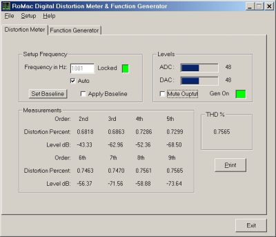
or http://shmelyoff.nm.ru/ -
I thought the generator should have some form of frequency readout to make it more user friendly. Also many members will not have a frequency counter making it difficult to set the frequency.
Driving LCD's is quite easy, so this was the obvious way to do this.
I used a PIC16F628A for this design. Why? Because I have them and use it a lot. With the 4MHz clock it will read up to 25kHz with 1Hz resolution. For best accuracy the crystal frequency should be measured and adjusted with aid of a frequency counter.
The diagram posted is with the add on modifications (inside the green box). The last diagram shows the green box expanded for better view.
If you don't want to build the counter section, then just build the circuit in the previous post.
I also uploaded the Counter.hex (Counter.zip) file so you can just program, or get someone to program the chip for you.
Hope members find my design useful :) -
Nobody should be without a function generator.
I know there are chips that you can use, but it is still good to learn how these things work.
The stand alone chips have very limited output power and the lower spec parts may have quite high sine wave distortion.
Here is a design I did using one of my previous posted ideas. That is the triangle to sine converter based around Q1.
http://www.electronics-lab.com/forum/index.php?topic=7405.msg59625#msg59625
Well in short, U1,2 is a comparator-integrator combination to provide square and triangle wave outputs on pin 1 and 7. Frequency is set in 3 ranges with R6 and (C1,2,3). R8 set the output level of the triangle wave to 8Vp-p at pin 7(U1B). Due to resistor tolerances, R8 might need slight adjustment to set the level at 8Vp-p on this pin. This level is important to get lowest sine distortion from Q1.
This triangle wave is then converted by the circuit around Q1 to a sine wave output at about 2Vp-p. R3,5 will be adjusted for minimum sine wave distortion. The values indicated in (%) were the settings for minimum distortion during simulation.
U2 plus D3,4,5 and Q2,3 forms a low distortion output stage. This output is capable of driving 10Vp-p into 600 Ohm load or around 8Vp-p into a 50 Ohm load. R11 will adjust the output level. Output stage distortion is only 0.002% at 20kHz with 10vp-p into 600 Ohm. The figure with 8Vp-p into a 50 Ohm load is 0.087%
Switch J1 when opened allows us to set the DC offset of the output. In the closed-cal position, the offset will be very close to 0V.
Design shows good performance with sine wave distortion only 0.7% THD at 20kHz
Up to 2kHz, distortion is about 0.35% THD, and then rising slowly to the 0.7% mark at 20kHz.
Although this circuit as a whole was only tested on a simulator, I have previously verified performance of the tri-sine converter and the output stage design on a bench with actual measurements.
Waveforms show the simulated results to expect at 20,200Hz and 2,20kHz.
From the table of %THD we see that the design perform well with 50 and 600 Ohm loads. -
Power in SMPS will be mainly limited by:
Effective core area
Switching frequency
Core loss at switching frequency vs peak flux swing
Copper loss
Switching losses of the active device
Rectifier losses -
Just to explain the concept of negative resistance. If we take the transistor circuit without the crystal connected and use a NWA to look at the real part of the input impedance (red) and available gain (blue), we can see that our values generate the plots as shown.
We can see that the red curve indicates that the circuit will have a negative resistance of about -58 Ohm (this more than cancels our +50 Ohm from RS) at 5MHz. We also see that the gain is near maximum at 5 MHZ confirming potential for oscillation as soon as we add the tuned circuit (crystal).
It is also clear that if we had a crystal with a RS of around 10 Ohm and frequency at 9 MHz, the circuit will not have enough gain (gain < 1 at this point) with our present capacitor values to oscillate.
The last plot show the result of increasing the capacitor values. We still have enough gain, but now we have only -40 Ohm negative resistance and not enough to cancel RS.
-
Here is a conventional diagram
http://www.eserviceinfo.com/downloadsm/27009/Daewoo_KOR-180A2A,%20KOR-181G2A,%20KOR-181H2A.html
Also http://www.repairfaq.org/sam/micfaq.htm
Many modern microwave ovens now use a HF, high voltage switch mode PSU -
You need a varmeter that measures the the product effective [(Voltage x Current) x Sin (angle between V and I)] . Reading will only obtained when V and I have a a certain phase difference. Readings for 0 deg and 180 degree phase difference will read zero.
-
Oxygen senser feedback is disabled while engine is still cold or full-throttle operation. Max power requires a rich mixture.
-
Recently a friend
-
I will stop discussion on this subject in the hope that I met with Mr. AN920 in another new subject. Thank you very much and goodbye.
Thank you for your kind remarks, but actually I am O+ who loves EE in a mainly <-O world. ;) -
To get the values of LS,CS, RS and Co
Measure the points Fs and Fp very accurately. Use narrow span on NWA
Measure holder capacitance Co with LCR meter at low test frequency (1-5kHz)
Then:
CS = Co{(Fp/Fs)^2 -1}
LS = 1/{[(2*pi*Fs)^2]*CS}
RS = {2*(NWA impedance)*[10^(insertion losses/20)-1]}; NWA impedance normally 50 or 75 Ohm
Insertion loss will be what you read for Fs on the MAG display in dB below 0dB. This loss will increase with increasing crystal Q values.
From this you can complete your model. It is handy to write a mathcad program to calculate all his if you are going to use it a lot.
It is possible to do this with a signal generator and a scope as well (will take much more time and not so accurate) as long as they have the same input and output impedances. Many better scopes have a 50 Ohm input selector and most RF generators are near 50 Ohm over their full frequency range. The scope must have a bandwidth much higher (5-10 times) than the Fs and Fp levels you are trying to measure. You will have to convert your relative display readings to dB. -
(a) That is the same as: SQRT(RS* DC gain) = SQRT(50 * 100) = about 70 (correct me) yes
(b) What this value? I mean what does that mean? Get ratio for loop gain vs C1, C2 values needed to be able to oscillate with given RS
Now lets discuss about some relevant points :
(1)The Crystal examiner that we are discuss about it. I built it to check for one type of crystal which is 455KHz. Here is its image:
from: http://www.ersatzteile-onlineshop.de/gruppen/3853000000-1.htm
All the remote controls that They were supposed to do repair containing this type.
When i get its model data LS, CS and RS, I'll redesign the original circuit according to the method you provided me and put it here for comments and corrections.
(2)Some sources have labeled them Resonator and others said crystals, Is there any difference? Uses ceramic materials instead of quartz. Q values not nearly as high as quartz but much higher than a normal LC tuned circuit. Model is the same
(3) I understand easily what resistor do in a circuit, also the cap and coils, but i can't imagine How crystal functioning in electronic circuit? It is a tuned circuit with L and C values, but with very high Q
(4) When I asked my first question on this topic, the circuit did not operate because of the error in the wiring but after correcting the error it worked well.
I kept some of the damaged crystal because I noted that some of the damaged crystals back to work after a period. I noted that by coincidence.
What I want to say here that I also noted that the testing device glows strongly with the good crystal quality and lighting weak with bad crystal.
From all of the foregoing Can I say that the crystal does not destroy just like transistors (0 or 1) it weaken or its condition worsened. Crystals and resonators can become lazy or damaged. Dropping quartz crystals on a floor is not a good idea, because the quarts wafer becomes very thin and fragile at high frequencies. They can also become damaged by very high drive level current through them which increases the internal dissipation
(5) The last question: I have heard repeatedly that the "remote control" pattern working with the carrier wave of 40 kHz, why use Crystal written on it 455 kHz? 455KHz resonators is used in radio IF circuits as well and cheap. They divide this frequency to get the 40kHz. The controlling micro can also be clocked by the 455kHz
Thank you very much -
(a)It was difficult to obtain any information from the seller in my country. How can measure these parameters by network analyzer?
I will provide a method for you later. Your network analyzer should be able to accurately measure Fs and Fp
(b) Do you not see that the value of Ls = 0.08H is very large value?
Yes, this is one of the characteristics of crystals, Large LS and small CS
(2)
Higher Q values will give better stability crystal.
Can you shed more light on this point and the relationship between Q and stability?
The higher the Q the more rapid the rate of phase shift vs frequency, meaning that the frequency have narrow margin for drift in short term. Long term drift may still occur due to temperature, aging and power dissipation in the crystal.
(3)
Step 4: Make sure transistor is biased at collector current that will give highest Ft. From the datasheet of BC182 we see that we can get this with a collector current of about 10mA. We will use a DC gain val of 100 with this transistor.
From datasheets i found:
Yes we have more ft (200 MHz at 10mA) than at 0.5mA, and this is more clear with the following graph:
Now, At Ic =10mA, DC hfe = 100 as shown in the following graph. Why you take the DC hfe not AC hfe?
The equation takes into account the calculation of amount negative resistance generated by the transistor by using DC gain, which is needed for oscillation to occur.
(4)
Select R1 to have about 50% of V1 on emitter.
In other words, you want to say that: Make VCE = 50% of V1?
Yes more or less, not very critical.
(5)Calculate R2 to give about 10mA collector current. Check that this value is at least (200 x RS, the higher, the better) for minimal loading on crystal.
Lets calculate it:
Vcc=9V, hfe = 100, VE = 4.5V and Ic = 10mA ==> IB = 10m/100 = 100uA
Vcc - RB*IB - VBE - VE =0
VBE at IC = 10mA (from one of the graphs in the datasheets) = approx. 0.68 V, so:
9 - 100u * RB - 0.68 - 4.5 = 0
RB = (9 - 0.68 - 4.5)/100u = 38.2 K ohm (far from 82 K)???
AND note that if IC = 10 mA then VE = 5.6 V not 4.5V. Please I want further clarification.
Correction : Rs * 200 = 50 * 200 = 10 K , yes you are right 38.2 K > 10 K
Yes, that is the calculated value but depends on the param or transistor self. Transistors from Philips will be different to say Motorola's. It is wise to verify the Ic finally and readjust Rb to get correct Ic. In my case I just simulated the circuit and with 39k resistor and BC182 model Ic was about 13mA. I increased Rb and Re to bring it down to 10mA. You don't want Re too low as it will reflect back to the base terminal x gain and load the crystal too much.
(6)
Check that this value is at least (200 x RS, the higher, the better) for minimal loading on crystal.
How a low value of R2 can load the crystal, please Explain this point.
R2 will appear in parallel over the crystal with the transistor input impedance reducing the Q of the crystal. -
I think it should trace out to be something like this. The 24VDC is further regulated down by another zener on the sensor pcb by the looks of it. You should be able to apply your 24VDC at the point indicated after removing Q1, or 24VAC by removing C4 and making R3 small enough or short out (should have about 28VDC over C1) to have a regulated 24 VDC over C3
They may also run the relay coil positive direct from the unregulated DC, just after the rectifier. I have seen both methods used. In this case the zener may only regulate the output voltage to 12VDC and not 24VDC -
Mathematical analysis of the usual Foster-Seeley and ratio detectors reveal a problem. To have very good reproduction of the modulating signal the split secondary winding should have equal properties. This is very difficult, if not almost impossible to achieve in real life. The slightest mismatch will introduce some distortion. The pulse-count detector eliminates this problem.
Later quadrature detection also tried to solve this problem by having only a single tuned circuit, but created another problem that a unwanted 2nd harmonic gets generated. -
One way to this is to use a technique called least-squares compression. It compresses the data in a time frame to allowed it to be read out at a lower data rate. Search Google for more information.
This is often used in simulation programs to speed up processing and optimization of results. -
The max CB voltage rating is higher than the max CE voltage rating because leakage current turns on the transistor at high CE voltages. Then the transistor would short the supply and melt. The leakage current is low enough so that CB voltage can be higher.
The collector Vceo implies the breakdown c-e rating with the base connection open. Transistors are hardly ever used like this, as normal operation always requires the b-c junction to be reverse biased. With reverse bias the c-e breakdown rating can be as high as 3 x Vceo. Designers like to use the Vceo rating because it has a automatic safety factor added.
The Oscilator projects
in Projects Q/A
Posted
I have not tried darlington's but due to their structure they will be very much slower in switching if they switch in this mode at all. I have a feeling they won't work.