
vbsemi
-
Posts
19 -
Joined
-
Last visited
vbsemi's Achievements
")


-
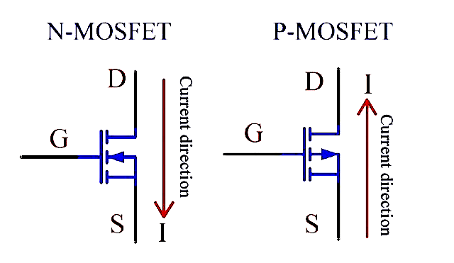
https://youtu.be/VUzMrbIt-Kw 如何识别三个终端: 我们知道 MOSFET 有三个端子: 门 (G):门最容易识别。 源 (S):无论是 P 沟道还是 N 沟道 MOSFET,相交线都表示源极端子。 漏极 (D):无论通道类型如何,具有单引线的一侧是漏极端子。 这三个端子用于连接外部电路。 G(栅极):通过改变电压电平来控制 MOSFET,从而直接导通或关闭 MOSFET。 D(漏极)和 S(源极):这些端子用作开关电路的两端,一端连接到电源,另一端连接到地。 如何区分 N 沟道和 P 沟道: 很简单,看看这个符号就知道了: 如果箭头指向栅极以外的位置,则它是 P 沟道 MOSFET。 If the arrow points toward the gate, it's an N-channel MOSFET. Direction of the Parasitic Diode: If the arrow of the parasitic diode points from the source to the drain, it's an N-channel MOSFET. If the arrow points from the drain to the source, it's a P-channel MOSFET. This parasitic diode plays a crucial role in circuit isolation. It helps in over-voltage protection by conducting excess current to the ground, preventing MOSFET damage. It also protects the MOSFET when the source and drain are reversed or when reverse-induced voltage occurs in the circuit. Once you understand these basic principles, using MOSFETs becomes much simpler.


-
 With the continuous advancement of automotive electronics technology, the Instrument Control Unit (ICU) serves as a crucial module in automotive electronic systems, responsible for processing and displaying key vehicle information. To meet the high demands for efficiency and reliability in modern vehicles, the ICU module requires superior performance in power management and switching control. The VBE1638 MOSFET, launched by VBsemi, provides an ideal solution with its excellent electrical characteristics, significantly improving the efficiency of signal processing and power management in ICU modules. Efficient Power Management The ICU module must achieve stable power management under various load conditions, and the VBE1638, with its 60V drain-source voltage and maximum drain current of 45A, meets the demands of high-power applications. Utilizing advanced trench technology, it reduces on-resistance (with a typical value of only 25mΩ), which minimizes power loss, enhances power management efficiency, reduces heat generation, and extends the lifespan of the device. Precise Signal Processing Precise signal processing is critical in automotive ICU modules, especially when dealing with complex sensor data. The VBE1638 MOSFET, with its low threshold voltage of 1.7V, enables quick response, ensuring the circuit can switch rapidly and adapt to different working states. Its +20V gate-source voltage (V<sub>GS</sub>) ensures high reliability and stability in various driving environments. Robust Thermal Performance The automotive environment is highly demanding, requiring ICU modules to operate stably over long periods under high temperatures, vibrations, and current fluctuations. The VBE1638, packaged in a TO252 casing, offers excellent thermal performance, effectively preventing overheating in high-temperature environments, ensuring long-term stable operation, and reducing vehicle system maintenance costs. Application Advantages The VBE1638 MOSFET is widely used in automotive instrument control unit modules, with optimized power management and power control performance ensuring reliable operation under varying load conditions. Whether in power management systems or complex control scenarios, the VBE1638 delivers stable and efficient performance. Product Specifications Model: VBE1638 Package: TO252 Polarity: N-channel Drain-Source Voltage (VDS): 60V Gate-Source Voltage (VGS): +20V Threshold Voltage (Vth): 1.7V On-Resistance (RDS(on) @VGS=4.5V): 30mΩ On-Resistance (RDS(on) @VGS=10V): 25mΩ Maximum Drain Current (ID): 45A Technology: Trench Other Applicable Areas Power Tools: In the power tool sector, such as drills and hammers, MOSFETs provide stable power output. With its high current-handling capacity and low on-resistance, the VBE1638 is an ideal choice for these modules, ensuring high efficiency and stable performance under heavy workloads. Industrial Automation: The VBE1638 is suitable for industrial automation equipment, including PLC controllers and motor drivers, supporting efficient automation and continuous innovation in smart manufacturing systems. LED Lighting: In LED lighting applications, the VBE1638 is used in LED driver modules, providing stable and efficient power support, ensuring long life and low energy consumption for LED lamps, streetlights, and landscape lighting products. As a high-performance MOSFET designed for automotive instrument control unit modules, the VBE1638 excels in power management and signal processing. Whether in complex signal processing scenarios or high-load power management, it helps enhance the overall efficiency and stability of ICU modules. As automotive electronics continue to evolve, the VBE1638 will play a vital role in more automotive applications, contributing to the innovation and upgrading of automotive electronic systems.
-
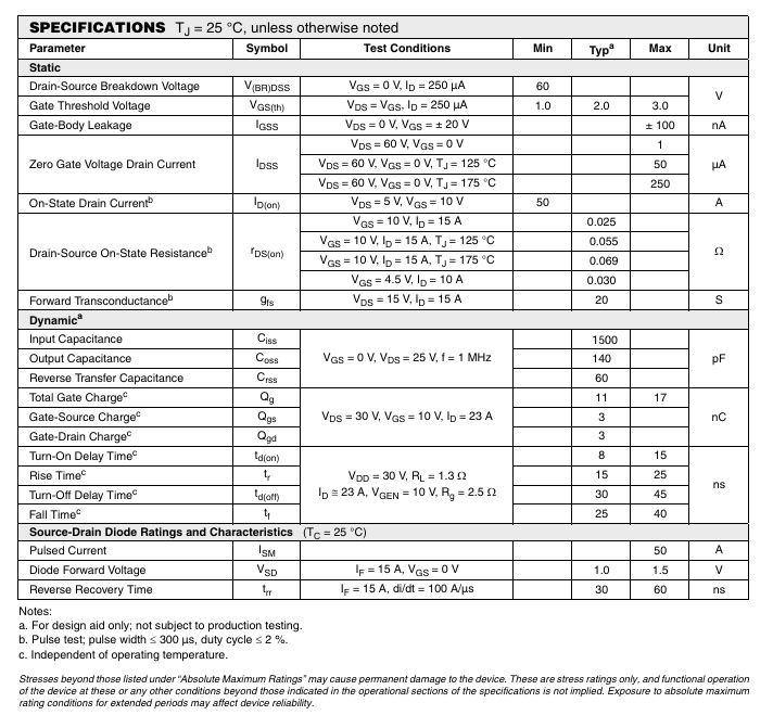
https://youtu.be/pbz5aMdxSEU 首先,微控制器 I/O 端口的负载能力有限,通常允许的电流约为 10-20 mA。因此,它们通常不用于直接驱动负载。 让我们简要比较一下驱动 BJT 和 MOSFET 的差异。 双极结型晶体管 (BJT): BJT 是电流控制器件。只要基极-发射极电压 (Ube) 超过阈值电压(通常为 0.7V),晶体管就会导通。对于 BJT,3.3V 肯定大于 Ube,基极电流 (Ib) 可以计算为 \( Ib = \frac{(VO - 0.7V)}{R2} \)。通过将适当的电阻器与基座串联,BJT 可以在饱和状态下工作。微控制器通常以低功耗为目标,因此电源电压通常很低,约为 3.3V。 MOSFET: MOSFET 是电压控制器件。栅源电压 (Vgs) 必须超过阈值电压才能开启,一般在 3-5V 左右,饱和驱动电压为 6-8V,高于 I/O 端口的 3.3V。如果用 3.3V 驱动,MOSFET 可能无法完全导通或以部分导通状态工作。在这种状态下,MOSFET 具有高内阻,这限制了其处理大电流负载的能力,从而导致功率耗散增加和潜在的损坏。 因此,通常最好使用微控制器来控制 BJT,而微控制器又会驱动 MOSFET。为什么使用 BJT 来驱动 MOSFET?这是因为与 MOSFET 相比,BJT 的负载能力较低,因此适用于控制应用。MOSFET 可以直接驱动吗?虽然某些低功率 MOSFET 是可能的,但通常不建议用于较大的负载。

-
https://www.youtube.com/watch?v=czRugPWSqx0 How does the MOS acceleration and deceleration switch work? Take NMOS as an example. When the current flowing into the gate is increased, the MOS will be accelerated when it is turned on. When the current flowing into the gate is reduced, the MOS will be decelerated when it is turned on; when the MOS tube needs to be turned off quickly, the gate charge needs to be released faster, and the deceleration shutdown will decelerate the release. PMOS is the reverse process of the above. We understand the switching process of the MOS tube. When an NMOS is turned on, the gate is charged. When the Cgs charge is full, the gate will turn on the threshold. When the NMOS is turned off, the GS charge needs to be discharged. When the charge is discharged, the gate will turn off the threshold. This explains the fast switch and deceleration switch we talked about earlier. So what is its fundamental mechanism? In essence, it is related to the gate resistance of the MOS tube. Because the gate resistance directly controls the size of the gate current, the switching speed varies with the gate resistance value. And choosing the right one is very important. Different gate resistors can be used for different switching speed requirements of MOSFET. When the MOS tube is turned on, the gate resistors: R1 and R2 are connected in parallel, and R2 is closed when it is turned off, so that it can be turned on faster and turned off slower; or like this circuit, the MOS tube passes through the gate resistor R1 when it is turned on, and R1 and R2 are connected in parallel when it is turned off, so that it can be turned on slower and turned off faster. The turning on and off of MOS is a dynamic process. The control end and the gate level are the same during continuous off or on, but the control end and the gate level are different at the moment of turning on and off. The gate level changes slower than the control end level, so the different levels will cause the gate current to flow into or out of the gate. Increasing the gate resistance value will slow down the switching speed of the MOSFET and increase its switching loss. Reducing the gate resistance value will increase the switching speed of the MOSFET. This has actually been mentioned in the previous section about the selection of the size of the resistor. It is not recommended to use K-level resistors when controlling the switching speed. Common resistance values are 3.3Ω/10Ω/33Ω, etc. Some relatively large discharge currents can be achieved by selecting low output impedance MOSFETs or voltage devices, such as using accelerating diodes.


-
https://youtu.be/_Ej50qOi3xk How does the discharge MOS of a BMS break down? Why is the voltage higher in a BMS system than in a system? Before the MOS tube is shut down, a large current flows through the MOS tube to power the load, which is almost the same voltage across the load as the battery at each end. Because the current does not change much, the parasitic inductors L1 and L2 are like wires. When the MOS tube is turned off, the current of the inductor cannot change suddenly, so a loop is required to maintain the current, and the inductor becomes a small power supply. The energy previously stored in the inductor requires the release of an electric current, but the current creates a voltage on the inductor. In other words, this circuit (including the battery) has three power supplies connected in series and applied to the MOS tube. Therefore, this total voltage must be higher than the battery voltage. How much taller is it? The L2 inductance is generally related to the positive and negative poles of the battery and the leads of the BMS system, and the parameters are generally relatively small; L1 inductors are different. In the case of over-current protection and short-circuit protection, the current is relatively large when the current is turned off, and the voltage drop will be large enough to penetrate the MOS transistor. How to solve it? You can make the MOS tube close slower, so that the di/dt will be much smaller and the voltage on L1 will be lower.


-
https://www.youtube.com/watch?v=ocE5HLg8E8E What is the function of the pull-down resistor on the of a MOSFET? The pull-down resistor between the gate (G) and source (S) of a MOSFET serves several functions: 1.Preventing False Turn-On: The Miller capacitance, a parasitic capacitor between the gate (G) and drain (D), can cause the MOSFET’s drain-source voltage (Vds) to change from nearly 0 (saturation voltage drop) to the bus voltage when the MOSFET is turned off. This rate of voltage change is "dv/dt." Since a capacitor responds to voltage changes by generating a current, the voltage change across the capacitor generates a current "i." The gate-source (G-S) junction has an insulating layer, usually silicon dioxide (SiO2), making G-S a high-impedance path (tens to hundreds of megaohms). If there is a driving abnormality, the current through the Miller capacitance can charge the G-S junction. A small current through a high impedance can correspond to a high voltage, potentially charging the gate voltage above the threshold voltage "Vgs(th)," causing the MOSFET to turn on again, which is a dangerous situation. 2.Providing a Discharge Path: In a flyback power supply topology, the Miller capacitance current is discharged through a low-resistance path inside the driver chip, preventing the gate from being charged high enough to cause a false turn-on. Here, we understand that there is already a discharge pull-down resistor inside the driver chip. However, if the gate resistor (Rg) is open-circuited or not connected for any reason, the external pull-down resistor (R8) can provide a discharge path for the Miller capacitance, keeping the G-S junction of the MOSFET at low impedance for a stable and safe state. This is a critical function of the pull-down resistor. 3.Pre-Protection Resistor: Another function of the pull-down resistor is as a pre-protection resistor. The G-S junction of a MOSFET is high-impedance, which is why it is sensitive to ESD. High voltage applied to the gate is not easily discharged and, over time, can damage the silicon dioxide layer between the G-S junction, leading to device failure. Therefore, the pull-down resistor balances power consumption and effective discharge. Typically, for low to medium power supplies (0-500W), a resistor value of around 10K-20K is chosen, while for high-power supplies, 4.7K-10K is selected.


-
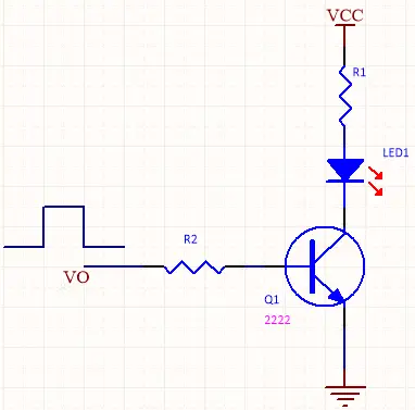
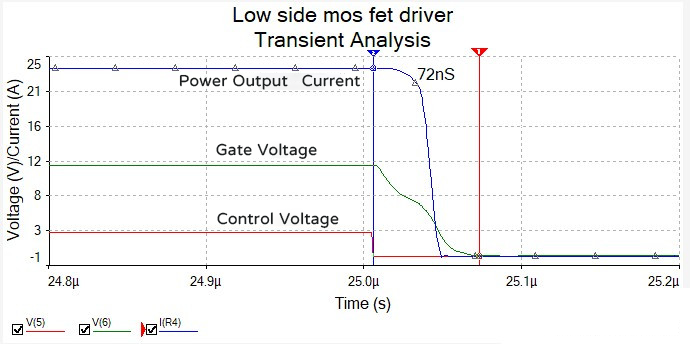
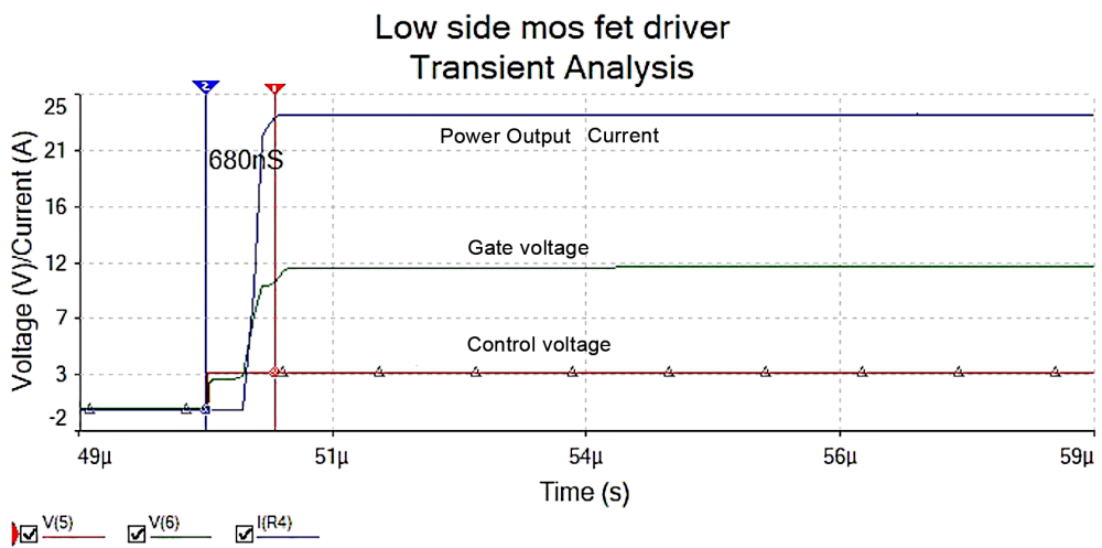
https://www.youtube.com/watch?v=CTJ2eVMSQaA 虽然 MOS 是电压驱动的,但栅极和源极之间存在较大的结电容。当它打开时,需要大的充电电流,当它关闭时,需要大的放电电流。因此,需要一个低阻抗的充电和放电路径。 这是一个低侧 MOS 管驱动电路。输入端由 Q3 和外围组成,使用公共基极连接形成一个电平 转换电路。控制输入从 (5) 接收,控制输入可由 MCU 生成。输入 3V 转换为输出 12V。由于 Q1 Q2 是互补发射极跟随器,因此不存在 Q1 Q2 同时导通以短路电源的问题。为了防止事故发生,在输出端串联电阻器是一种安全的做法。 The time required for MOS to turn on from off to on is longer than the time from on to off. Reducing R1 can shorten the time from off to on. But it is not unlimited because the current pulling capacity of the driving source is limited. When the control voltage changes from low to high, there is a 3V step at the beginning of the gate voltage. Analysis shows that it is caused by the 3.3 bias voltage feeding through the BC junction after Q3 is turned off. In the switching state, the MOS tube needs to be closed and opened as quickly as possible, and this circuit can effectively control it.
-
https://www.youtube.com/watch?v=pWDCny75LrA Pull-up and pull-down resistors are essentially resistors. They are called pull-up and pull-down because they are used in different scenarios. For example, in a real circuit, we often encounter a situation where the output voltage amplitude of the device is insufficient. If the pre-amp can only output a level of 0V-3V, and the background system needs a high or low level of 0V-5V, a pull-up resistor can be used to force the output voltage of the pre-amp to be pulled, but this method can only pull the voltage up to between 3V-5V. Similarly, when the output low is not low enough, a pull-down resistor can be used to lower the low level. As for how much voltage can be pulled, it depends on the resistance value of the resistor. In the switching power supply of the MOS transistor, a pull-down resistor is generally added to the NMOS transistor and a pull-up resistor is added to the gate of the PMOS transistor, which is about 10K. It typically plays three roles: 1. Determine the level of the MOS tube gate 2. Prevent electrostatic breakdown 3. Provide an emission pathway When the MOS tube is powered on, it will be in a high-resistance state for a period of time. When it is turned on, this state is uncontrolled. NMOS may be interfered by high-frequency interference, and PMOS may be interfered by low-frequency interference, which can easily cause the switch tube to burn out. At this time, adding resistance can make the gate a certain level and no longer a high-resistance state. That is to say, the MOS tube will remain in a closed state when powered on until the microcontroller controls its switch. In addition, it is easy to accumulate some electrostatic charge when it is in a high-resistance state. When it reaches a certain level, a high voltage will be formed between GS. The MOS tube is easy to break down and be damaged, and a resistor is also needed to fix the level. We have talked about providing a discharge path before. The reason is that there is a parasitic capacitor in the GS of the mos tube. The resistor provides a discharge path for the parasitic capacitor when the power is off.


-
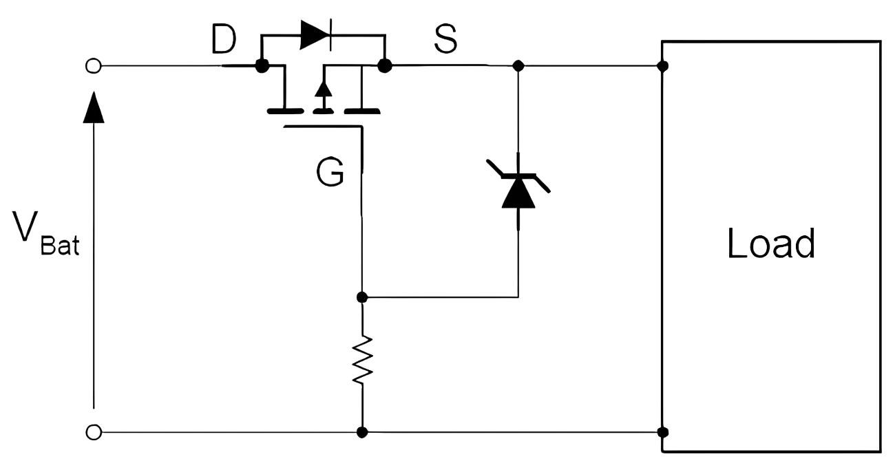
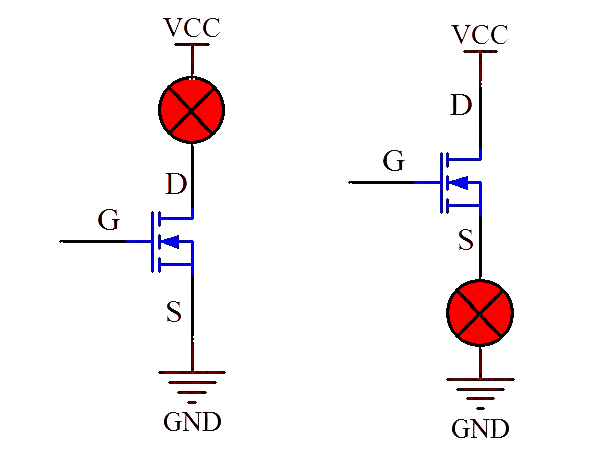
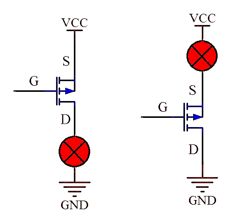
https://youtu.be/A7Q4pJbKY3k 有人说 NMOS 可以用作电路应用中的上管或下管。哪个更好?两者有什么区别? 众所周知,NMOS 和 PMOS 的电流方向相反,Vgs 具有一定的电压差。但是,NMOS 的 G 电位高于 S 电位 (5~10V),而 PMOS 的 S 电位高于 G 电位 (-5~-10V)。 这里,以 5V 的导通电压差为例,当使用 NMOS 作为下管时,S 极直接接地,将其固定到 5V 即可开启 G 极电压。 NMOS 如果用 NMOS 作为上管,D 极接正电源,S 极的电压不固定,则无法确定控制 NMOS 导通的 G 极电压,因为 S 极对地的电压有两种状态, MOS 管切断时为低电平,导通时接近高电平 VCC。但是,当 NMOS 用作上管时,控制电路会更加复杂。在这种情况下,必须使用隔离电源进行控制。改用 PMOS 会简单得多。 PMOS 使用 PMOS 作为上管时,S 极直接连接到电源 VCC,S 极电压是固定的,G 极电压只需要比 S 极低 5V 即可导通;同样,如果用 PMOS 作为下管,D 极接地, S 极电压不固定,无法确定控制极 G 极的电压,使用起来比较麻烦,需要隔离电压设计。 因此,在电路中通常使用 PMOS 作为上管,NMOS 作为下管。
-
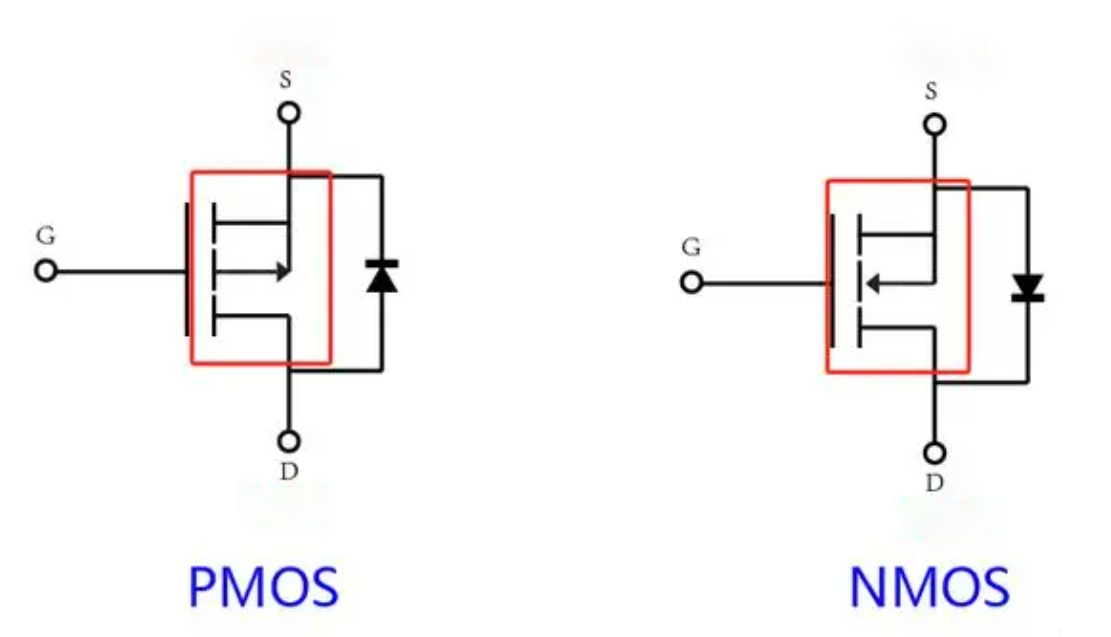
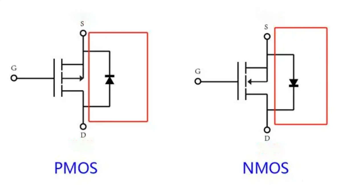
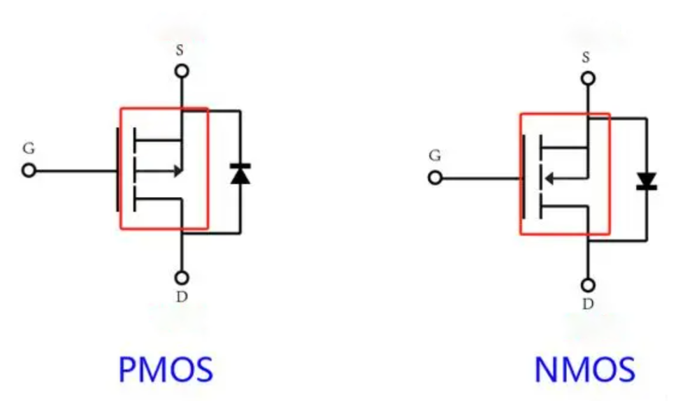
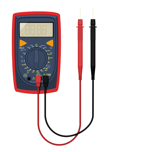
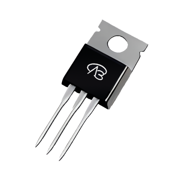
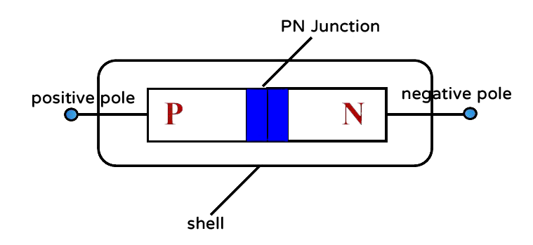
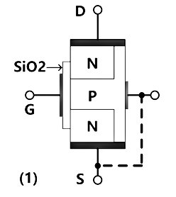
https://youtu.be/3e6fPoQ17wM 如何区分你手中的管子是N管还是P管? 首先,我们以增强MOS管为例。这是两者的电路符号: 您可以看到两个箭头的方向不一致。 这个箭头就是它的衬底,因为MOS管的内部衬底和源是连接在一起的。 NMOS和PMOS电路符号之间的最大区别在于其基板。NMOS的箭头指向闸门,而PMOS的箭头则指向闸门。 该箭头的方向与内部衬底与MOS管的通道逆温层之间的PN结方向有关。 其次,NMOS和PMOS的体二极管相反。 NMOS管的体二极管的阳极(即正极)连接到源极,PMOS的体二极管的阳极连接到漏极,体二极管的负极连接到源极。 那么,如何区分MOS管的三个引脚呢? 您可以使用万用表进行测试。下面简单说明一下。 拿一个封装为TO220的MOS管来说,它通常有一个散热片,散热片会连接到漏极。使用万用表测试哪个引脚可以连接到散热器,该散热器对应于漏极。 由于二极管的连接,漏极和源极之间存在二极管特性。 因此,当使用万用表测试漏极以及哪个引脚可以在正向和反向连接时,它就是源极。 剩下的就是大门了。 归纳起来,有两点: 1.NMOS二极管的正极一般接在源极上 2. 散热器连接到排水管

-
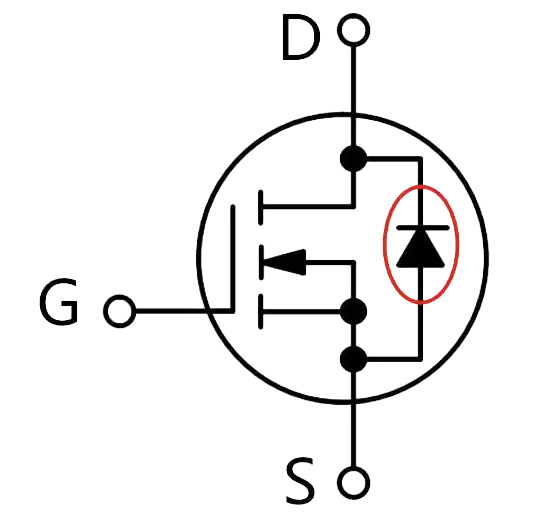
https://www.youtube.com/watch?v=pql2Ulae7mE MOS has a body diode connected in parallel between the D and S poles, so why is this diode connected in parallel? This starts with the process and structure of MOS. The diode is composed of a pair of PN junctions. The P-type region corresponds to the positive pole of the diode, the N-type region corresponds to the negative pole of the diode, and the PN junction is in the middle. SiO2 in the MOS tube itself is not conductive, so the driving pole G basically does not carry current. In addition to the three poles D, G, and S, there is also an intermediate pole, which is connected to the S pole, so in the circuit symbol of MOS, the arrow pointing to the channel N channel inside the MOS is connected to the S pole. In addition, the drain of the N-type region is connected to the middle P-type region and then to the source, which just forms a diode structure, so a diode is connected in parallel in the MOS symbol. What is the use of this body diode? In some scenarios, such as battery protection, after the lithium battery is over-discharged, the protection function will be turned on: turn off the discharge MOS. When the charger is plugged in, the MOS body diode is used to make the circuit conductive and the system work normally. However, in some scenarios, the existence of this diode is undesirable because it may cause leakage between the S pole and the D pole.
-
False Turn-On in MOSFET Driving Circuit and Countermeasures
vbsemi posted a topic in Theory articles
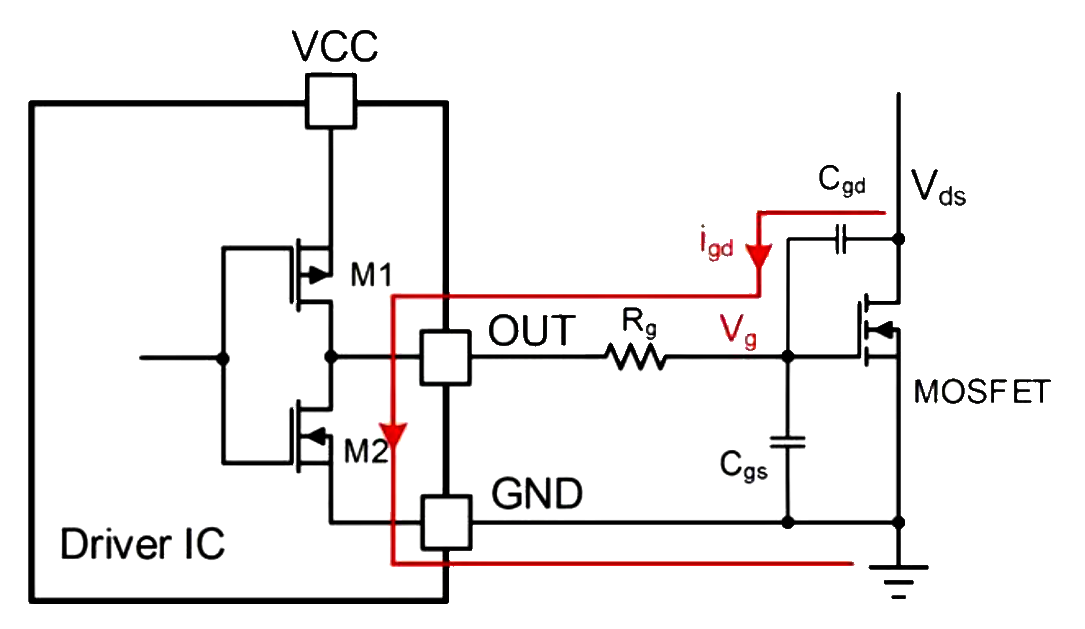
https://www.youtube.com/watch?v=PwOTTqUo9tA MOSFET is a switch controlled by gate voltage. When the gate voltage is greater than the turn-on threshold, the MOSFET is turned on; when the gate voltage is lower than the turn-on threshold, the MOSFET is turned off. In actual applications, due to the influence of other factors such as device and peripheral circuit parasitic parameters, the originally turned-off power device may be mistakenly turned on. Today, let's talk about the mistaken turn-on of MOSFET in the drive circuit and its countermeasures. Let's talk about two cases of mistaken turn-on: mistaken turn-on caused by Miller effect and mistaken turn-on caused by parasitic inductance. False turn-on caused by Miller effect When the MOSFET is turned off and then turned on, the Vds voltage (the maximum voltage that can be applied between the drain and the source) rises rapidly to produce a high dv/dt (the rate of change of the drain-source voltage during the switching transient), thereby generating a displacement current (igd) in the capacitor Cgd (Miller capacitor). This displacement current will generate a voltage spike after flowing through . If this voltage spike exceeds the turn-on threshold of the MOSFET, the MOSFET will be turned on, causing the circuit to be turned on or even damaged. Another type of false turn-on is caused by parasitic inductance on the line. As shown in the figure below, Ls is the parasitic inductance on the source of the MOSFET. When the MOSFET is turned off quickly, the current decreases rapidly to produce a high di/dt, and then a negative voltage (VLS) is generated across the two ends of the parasitic inductance. If this VLS voltage exceeds the gate threshold of the MOSFET, the MOSFET will be turned on by mistake. So, what methods do we have to deal with the phenomenon of MOSFET being turned on by mistake? 1. Adjust the gate drive resistor and capacitor The turn-on/off speed of the MOSFET can be adjusted by adjusting the size of the gate drive resistor and capacitor: increase the gate drive resistor and capacitor to slow down the turn-on/off speed of the MOSFET, reduce dv/dt (di/dt) and thus reduce the gate voltage spike. 2. Add a transistor A transistor can be placed near the gate of the power tube to prevent false opening during the shutdown period, effectively suppressing the false gate opening caused by the Miller effect. 3. Use an anti-parallel diode The current in the inductor can disappear through the diode loop, thereby avoiding the generation of reverse potential.
-
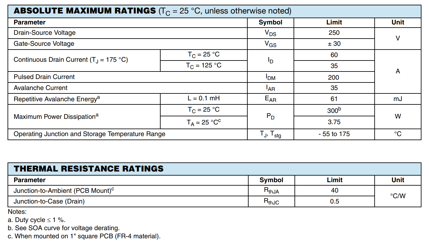
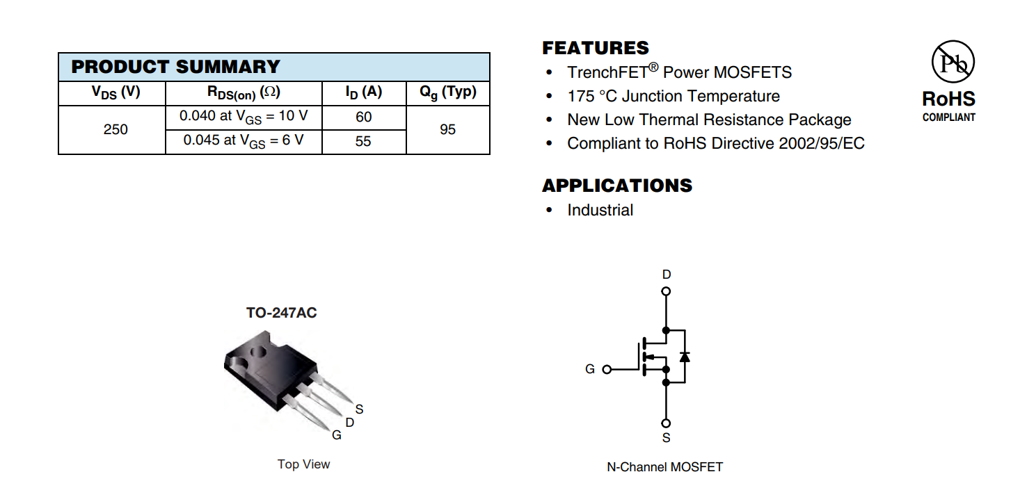
In the context of the current global energy transition, the utilization rate of renewable energy continues to increase. Clean energy such as solar and wind energy has become an important part of the energy structure. However, there are still challenges to the efficient conversion and storage of these renewable energy sources. VBP1254N MOSFETs were introduced by VBsemi because excellent performance and reliability were the key factors in solving these problems. High-efficiency inverter core The inverter is an important equipment that converts direct current into alternating current, and is widely used in solar power generation systems and wind power generation systems. The emergence of VBP1254N provides strong support for the efficient energy conversion of inverters. Its drain-to-source voltage (VDS) of 250V and drain-to-source current (ID) capability of 60A enable MOSFETs to handle high-power power conversion. In addition, VBP1254N uses advanced trench technology to provide low on-resistance (RDS(on)). When VGS=10V, the typical value is only 40mΩ. This feature significantly reduces energy loss, improves the conversion efficiency of the inverter, helps the system maintain low heat accumulation at high power output, and extends the life of the equipment. A reliable choice for battery management systems In renewable energy systems, battery management systems (BMS) are critical to the performance of energy storage devices. VBP1254N is a reliable choice for battery management systems due to its stable performance and high threshold voltage (Vth, 3.5V typical). MOSFETs can effectively control the current during charging and discharging to ensure the safe and efficient operation of the battery pack under different working conditions. Its ±20V gate-to-source voltage (VGS) feature enables VBP1254N to operate reliably under extreme conditions. This is particularly important for fast response and high reliability requirements in energy storage systems, ensuring that the system can quickly adjust the current under various load conditions, avoid overcharging or overdischarging the battery, and prolong the battery life. Application prospects and advantages The high performance of the VBP1254N makes it very promising for use in renewable energy systems. Whether it's an inverter or a battery management system, this MOSFET performs well. Its excellent performance in high-power energy conversion and energy storage applications perfectly overcomes the relevant technical difficulties and provides a solid guarantee for the efficiency and reliability of the energy system. Detailed parameter description 1. **Product model**: VBP1254N 2. **Package**: TO247 3. **Configuration**: Unipolar 4. **Polar**: N channel 5. **Drain-Source Voltage (VDS)**: 250V 6. **Gate-Source Voltage (VGS)**: ±20V 7. **Threshold voltage (Vth, typ)**: 3.5V 8. **On resistance (RDS(on)@VGS=10V, typ)**: 40mΩ 9. **Drain Current (ID)**: 60A 10. **Technology**: Trench 11. **Seamless replacement models**: IXTH50N25T, IRFP4229 Examples of other areas of application for the product 1. **Industrial Automation**: VBP1254N can be used for motor drives and control systems in industrial automation. Its high current handling capability and low on-resistance make it ideal for high-efficiency motor drives. Whether in factory automation equipment or robot control, the equipment provides reliable power transmission and stable performance. 2. Power Management:VBP1254N performs well in power management modules, especially in high-efficiency switching power supplies and DC-DC converters. Its low on-resistance and high threshold voltage ensure high efficiency and system stability for energy transfer, making it a high-efficiency power supplyA core component of the management system. High-performance devices designed to address high-power energy conversion and energy storageIssue. It not only improves the overall efficiency and stability of the renewable energy system, but also provides strong support for the further development of green energy. In the future, with the continuous progress of technology, VBP1254N will continue to give full play to its unique advantages in more fields to promote the innovation and application of energy technology.


-
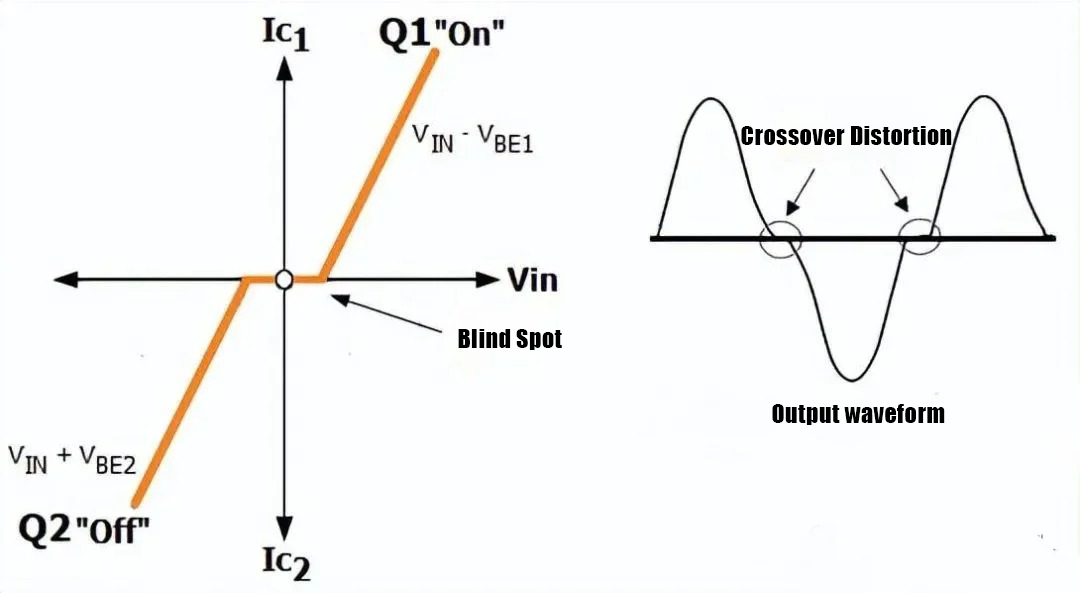
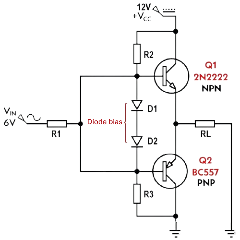
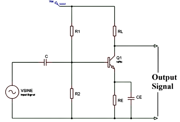
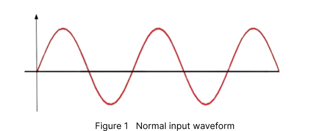
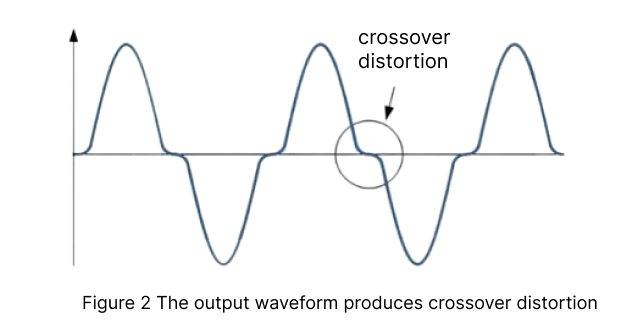
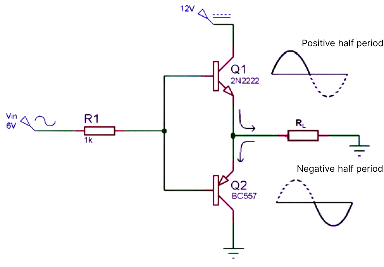
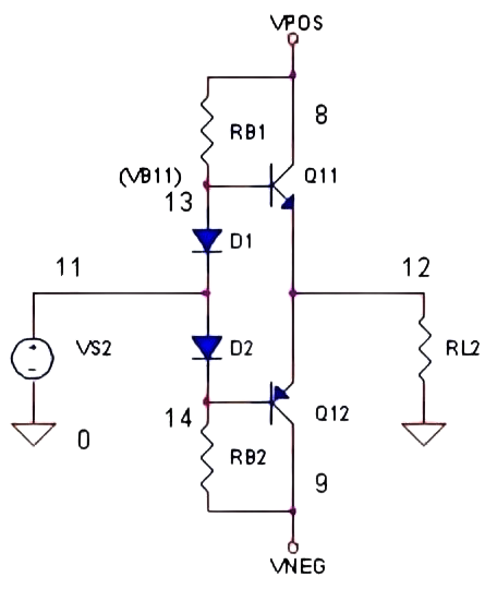
We know that push-pull circuits come in many types, such as class A or class B amplifiers. Class B amplifiers are the ones used in practical applications. They are more efficient than class A, but they are often affected by crossover distortion. So how does it affect it? How can it be reduced? When the signal is distorted at 0V, the transistor will provide a voltage of 0.7v at the base-emitter junction before turning on. When the AC input voltage is applied to the push-pull amplifier, it increases from 0 until it reaches 0.7V, and the transistor remains off without any output. So why does crossover distortion occur when VIN reaches zero? (Class B amplifier) In fact, transistors Q1 and Q2 cannot be turned on at the same time. If Q1 is turned on, VIN must be greater than Vout, and if Q2 is turned on, Vin must be less than Vout. If VIN is equal to zero, Vout must also be equal to zero. When VIN increases from zero, the output voltage Vout will also remain at zero. Until V IN is less than 0.7V, the output voltage shows a dead zone, and the same situation will occur when V IN starts to decrease from zero. How to reduce the crossover distortion of the push-pull transistor circuit? It can be corrected by using two diodes that are turned on at the transistor position, that is, the class AB amplifier circuit. It uses the characteristics of both. From 0V to 0.7V, the diode is biased in the on state to make up for the 0.7 V loss of the emitter follower. At this time, the transistor has no signal at the base, which solves the crossover distortion problem. In addition, it can also be achieved by reducing the resistance value. This is because the resistor RB1 controls the current of D1. The smaller RB1 is, the greater the current is, that is, the greater the voltage of the diode is, so when there is no input signal, the Vbe will be greater. This increased deviation will further reduce the distortion. However, the specific application situation is still based on the actual circuit design.


-
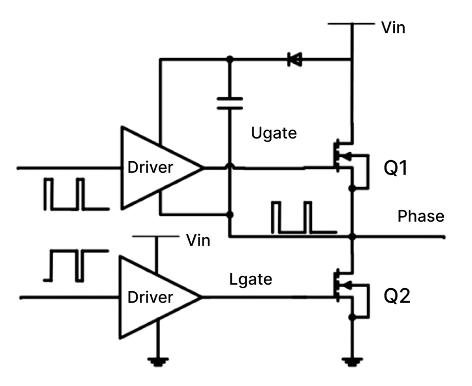
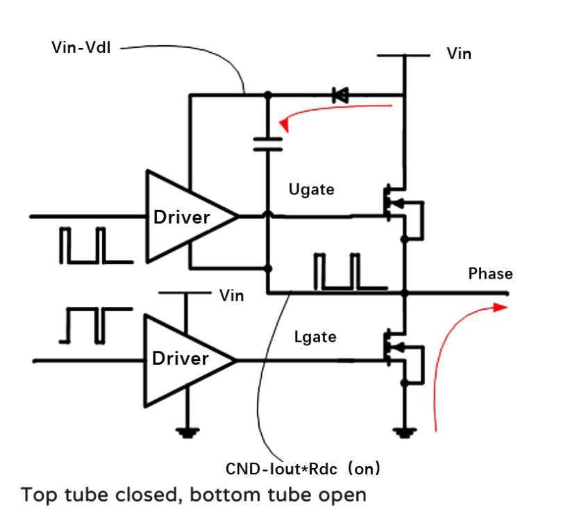
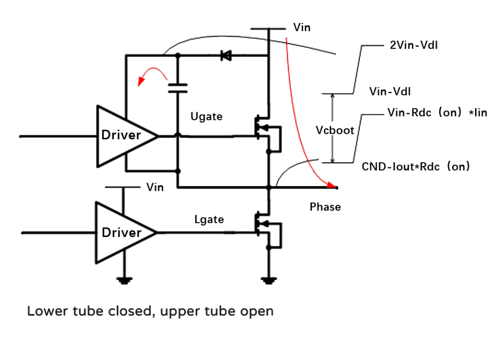
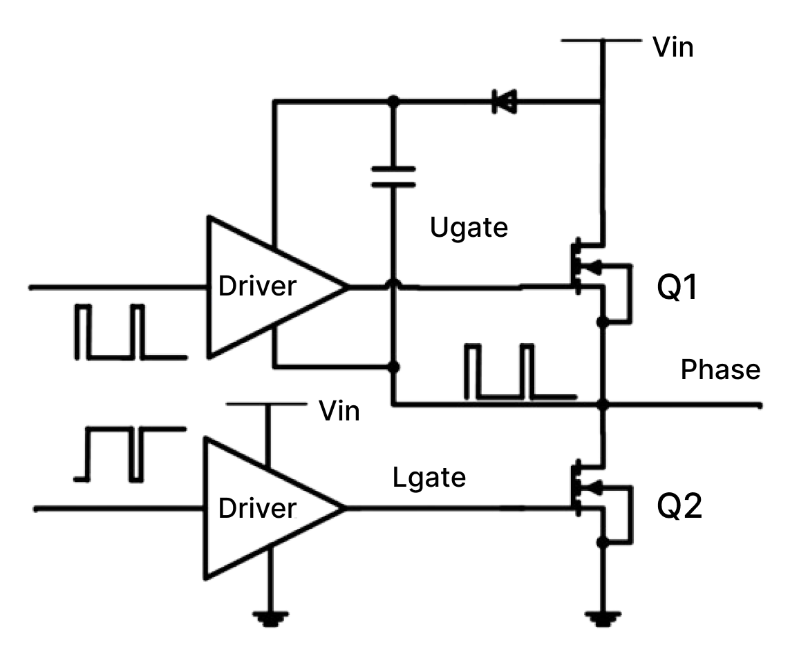
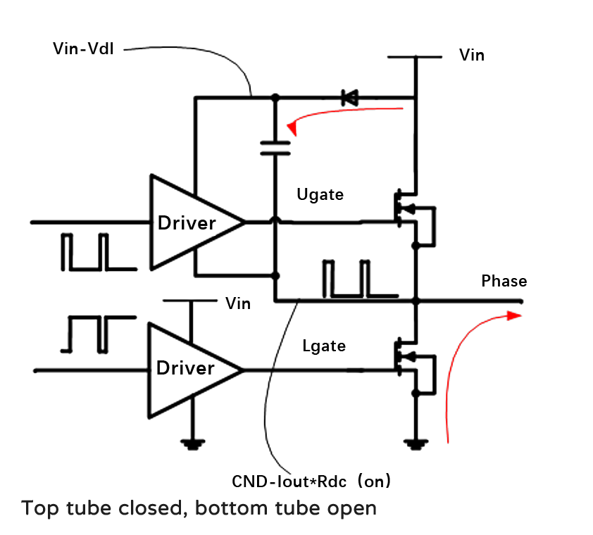
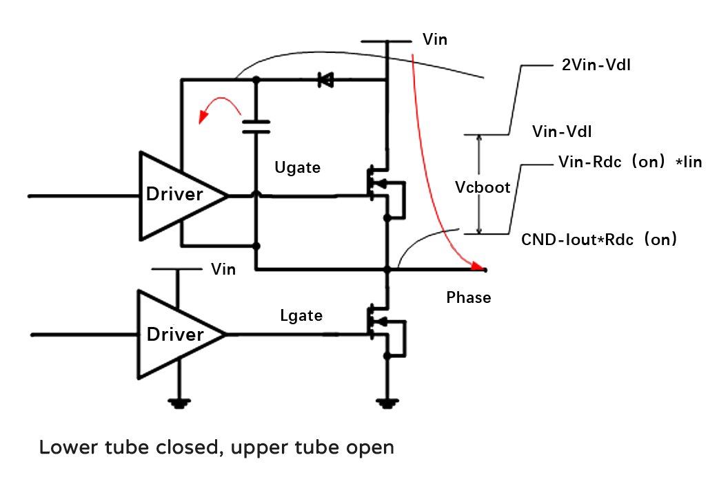
We know that the Buck circuit generally needs a "top tube" to control it, and this realization of raising its own voltage mainly depends on a capacitor, which is the bootstrap capacitor. So how does this capacitor achieve its function? For example, a small capacitor is connected between the GS of the MOS. The MOS charges the capacitor when it is not turned on. When the MOS is turned on, when the S-pole voltage increases, the power supply voltage of the driver above will be automatically increased. At this time, the output voltage of the driver also increases and is connected to the G-pole of the top tube. In other words, the G-pole generates high voltage, and there is enough voltage difference Vgs between the G-pole and the S-pole, so the top tube MOS continues to be turned on. During the charging process, the IC will prohibit the upper and lower tubes from being turned on at the same time to prevent direct conduction. In other words, the upper tube will be turned off and the lower tube will be turned on, and then the diode D1 and the bootstrap capacitor C1 will form a charging circuit. The input power passes through D1, C1, the lower tube, and finally to the ground (negative pole of the power supply), forming a loop to charge the capacitor so that the voltage on both sides of the capacitor is equal to the input power. Conversely, when the lower tube is turned off, the previous loop is naturally cut off, and D1 is in reverse cutoff. At this time, the capacitor will keep the voltage change continuous, and the Vc voltage will gradually decrease with discharge without sudden changes. However, during the charging process, since the capacitor has been charged, the Vc voltage is approximately Vin, so the Vgs of the upper tube is also equal to the input power supply, and this voltage is enough to turn on the upper tube. In this way, a PWM cycle is completed, which is the charging and discharging process of the bootstrap capacitor.