Jump to content
Electronics-Lab.com Community

Search the Community

Showing results for tags 'diy'.

  • Search By Tags

    Type tags separated by commas.
  • Search By Author

Content Type


Forums

  • Electronics Forums
    • Projects Q/A
    • Datasheet/Parts requests
    • Electronic Projects Design/Ideas
    • Power Electronics
    • Service Manuals
    • Theory articles
    • Electronics chit chat
    • Microelectronics
    • Electronic Resources
  • Related to Electronics
    • Spice Simulation - PCB design
    • Inventive/New Ideas
    • Mechanical constructions/Hardware
    • Sell/Buy electronics - Job offer/requests
    • Components trade
    • High Voltage Stuff
    • Electronic Gadgets
  • General
    • Announcements
    • Feedback/Comments
    • General
  • Salvage Area

Find results in...

Find results that contain...


Date Created

  • Start

    End


Last Updated

  • Start

    End


Filter by number of...

Joined

  • Start

    End


Group


Website URL


Yahoo


Skype


Location


Interests

Found 8 results

  1. In this project, we will design a simple yet powerful digital signal processing (DSP) system using the XCR3128XL-7VQ100C FPGA. This versatile and high-performance FPGA provides the ideal platform for implementing custom DSP algorithms. The project will focus on creating a basic signal filter, allowing you to gain hands-on experience in digital signal processing, FPGA development, and hardware design. Project Overview Digital signal processing is an essential aspect of modern electronics, especially in fields like audio processing, communication systems, and control systems. The XCR3128XL-7VQ100C FPGA from Xilinx is a highly configurable device, capable of handling complex logic and arithmetic operations needed for DSP applications. For this project, we will implement a simple low-pass filter on the FPGA, which is one of the fundamental operations in DSP. This project will involve: 1. Setting up the XCR3128XL FPGA on a development board. 2. Designing a low-pass filter using the FPGA’s logic resources. 3. Testing the filter with a real-world signal. 4. Understanding how the FPGA handles data processing for DSP applications. The FPGA will act as the heart of the system, processing incoming signals in real-time and applying the low-pass filter algorithm. Components Needed 1. XCR3128XL-7VQ100C FPGA: The main processing unit for this project, capable of handling multiple parallel operations efficiently. 2. Power Supply: To power the FPGA, a stable 5V or 3.3V power supply will be required, depending on the configuration of the board used. 3. Oscilloscope or Signal Generator: To test the functionality of the filter and visualize the input and output signals. 4. Signal Source: This could be any analog or digital signal source. A function generator can provide sinusoidal or square wave signals for testing. 5. Development Board: An FPGA development board that supports the XCR3128XL-7VQ100C chip. 6. Breadboard and Wires: For connecting the signal source, FPGA, and oscilloscope. 7. Optional Components: For interfacing, such as ADCs (Analog to Digital Converters) or DACs (Digital to Analog Converters), depending on your system's requirements. Step by step guide Step 1: Setting Up the FPGA The XCR3128XL-7VQ100C is a 3.3V FPGA with 128K gates and 128 I/O pins. These capabilities make it ideal for implementing signal processing tasks without overwhelming the FPGA’s resources. Select a Development Board: First, you will need a development board that hosts the XCR3128XL FPGA chip. A common choice might be an FPGA evaluation board with an integrated JTAG interface for programming. Ensure that the board has the necessary voltage regulators and level shifters for interfacing with external devices (like signal generators or oscilloscopes). Install Development Tools: To program the FPGA, you will need the appropriate software tools. Xilinx provides ISE Design Suite (Integrated Software Environment), which includes all the necessary tools to design, simulate, and synthesize FPGA circuits. Once installed, create a new project and set the target device to XCR3128XL-7VQ100C. Initial Setup: Power the FPGA development board and connect it to your computer via the JTAG interface. Use the Xilinx software to configure the FPGA and ensure that the device is correctly recognized. Step 2: Designing the Low-Pass Filter In this project, a simple FIR (Finite Impulse Response) low-pass filter will be implemented on the FPGA. The purpose of a low-pass filter is to allow low-frequency signals to pass through while attenuating high-frequency noise. The filter will take an input signal, process it in real-time, and output the filtered signal. The FIR filter design can be represented as a sum of weighted inputs, where the weights are the filter coefficients. In the FPGA, we will implement this using parallel adders and multipliers. Here’s how we can break the design into smaller tasks: 1. Input Signal Interface First, we need to interface the FPGA with an input signal. This could be an analog signal converted to a digital format using an ADC (Analog-to-Digital Converter). The digital signal will then be processed by the FPGA. 1. Signal Sampling: The input signal will be sampled at a fixed rate, typically 10 kHz or higher, depending on the signal characteristics and filter specifications. 2. ADC or Signal Generator: If using an external signal generator, the FPGA will receive the sampled data at the clock frequency and process it accordingly. 2. Filter Coefficients For a simple low-pass FIR filter, we’ll select a set of coefficients that define the filter's response. The coefficients can be calculated offline using filter design tools, but for simplicity, let's assume a basic set of coefficients like this: These coefficients represent the weights that are applied to the input signal samples. In a more advanced design, you would calculate these values based on the desired cutoff frequency and other parameters. 3. Implementing the Filter We will implement the filter using parallel processing elements in the FPGA. Each element will multiply the corresponding input sample by the filter coefficient and then sum the results. 1. Multiplication: For each incoming signal sample, the FPGA will multiply it by the corresponding filter coefficient. 2. Addition: The results of the multiplications will be summed together to produce the output signal. The FPGA will have a parallel processing structure that can handle multiple operations at once. This makes it suitable for high-speed, real-time processing tasks like digital filtering. 4. Output Signal The processed signal will be the filtered output. This signal can be sent to a DAC for conversion back to an analog signal, or it can be analyzed in its digital form. A digital-to-analog conversion may be necessary if you wish to output the signal as an analog waveform, which can be done using a DAC. Step 3: Programming the FPGA With the filter design in place, it’s time to program the FPGA. The process involves writing VHDL or Verilog code to describe the behavior of the low-pass filter. The code will define the filter's structure, the handling of input signals, and the output. Create the VHDL Modules: Start by writing VHDL code to define the modules that will handle the multiplication and addition for the FIR filter. You can create separate modules for the multiplier and adder operations to keep the design modular. Simulate the Design: Before implementing the design on the FPGA, simulate it using the built-in simulation tools in the Xilinx ISE suite. This will help ensure that the logic is functioning correctly and that the filter behaves as expected. Synthesize the Design: Once the design is verified through simulation, synthesize it to generate the bitstream file that will be used to program the FPGA. This step converts the high-level VHDL code into a configuration that the FPGA can understand and execute. Program the FPGA: Use the JTAG interface to load the bitstream file onto the XCR3128XL FPGA. Once the FPGA is programmed, it will begin processing input signals through the filter in real-time. Step 4: Testing the Filter Now that the FPGA is running the filter design, it’s time to test the system with a real input signal. Input Signal Generation: Use a signal generator to provide an analog signal to the input of the FPGA (through an ADC if necessary). A sine wave or square wave is ideal for testing the filter’s response. Monitor the Output: Use an oscilloscope to visualize both the input and output signals. You should see the filtered signal with high-frequency components attenuated and low-frequency components passing through. Adjust Filter Coefficients: If the output is not as expected, you can adjust the filter coefficients in the design. This might involve recalculating the coefficients and reprogramming the FPGA with the updated design. Fine-tune the System: You may need to fine-tune the sampling rate, filter coefficients, or other aspects of the system to meet the requirements of your specific application. Step 5: Finalizing the Project Once the system is working as expected, you can finalize the project. Some ideas for further improvements could include: 1. Implementing More Complex Filters: You can modify the design to implement higher-order filters or other types of DSP algorithms. 2. Real-Time Performance: Test the system under real-time conditions to ensure it operates efficiently at the desired sampling rate. 3. Interface Enhancements: You could add additional functionality such as a user interface for adjusting filter parameters or displaying output. Conclusion This DIY electronic project demonstrated how to use the XCR3128XL-7VQ100C FPGA to implement a basic digital signal processing system. We created a simple FIR low-pass filter, learned how to interface the FPGA with external signals, and tested the system using a signal generator and oscilloscope. FPGAs like the XCR3128XL-7VQ100C are incredibly powerful tools for signal processing, offering the flexibility and speed needed for real-time applications. By following this project, you gained valuable experience in both FPGA design and DSP, setting a foundation for more complex projects in the future.
  2. In this article/video, I used an RP2040 Zero board, a VL53L0X Laser time-of-flight ranging sensor, and a 2.4” TFT display to build a graphical laser rangefinder unit that can be used to monitor the distance, check the liquid level, etc. The board is also equipped with a relay and a buzzer that allow the user to provide distance-related acoustic signals or activate/deactivate an external device, such as a pump, brake, etc. Source: https://resources.altium.com/p/rp2040-zero-powered-laser-range-finder-gui-and-24-tft-display
  3. Hi, all I'm using a PCA9685 with a pinout board like Adafruit's. I'm trying to run a bunch of LEDs at 20 mA, and the chip is supposed to be able to source 10 mA and sink 25 mA. I understand that to have it Source, you connect the LED between the PWM and GND pins and to Sink you connect it between V+ and PWM. I've tried both ways and using a multimeter and a red LED I get 12.5 mA. Why is it not 25 in Sink? Also, why do I get 12.5 on Source mode as well? Is there anyone have ideas of it? if possible a simple explanation would be nice. Many thanks.☺️
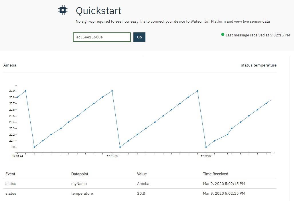
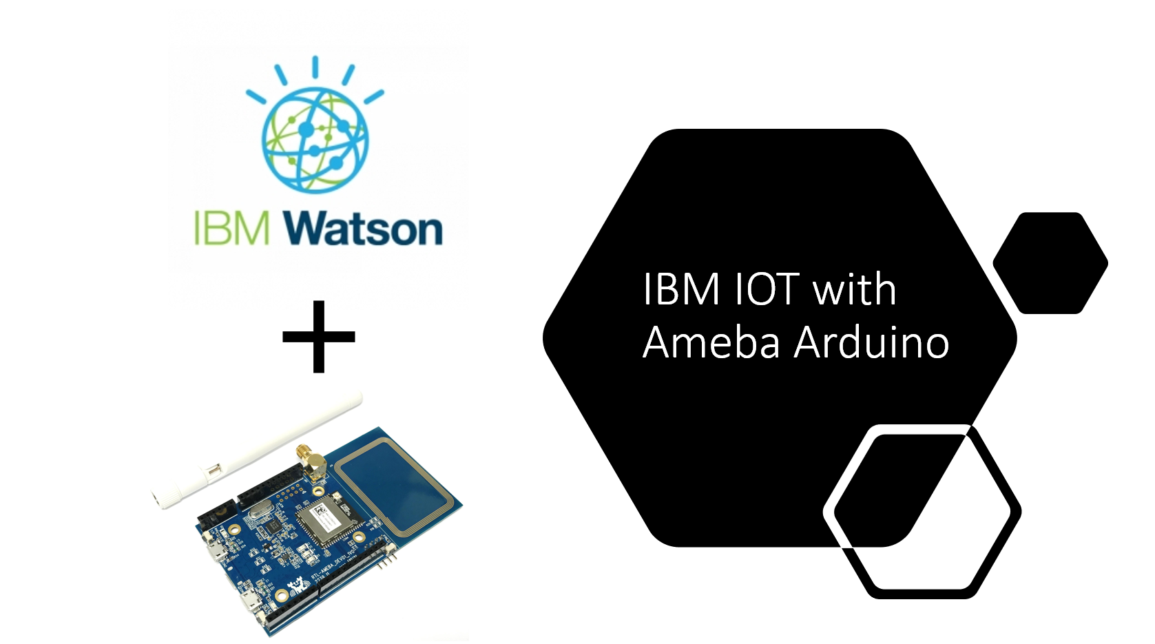
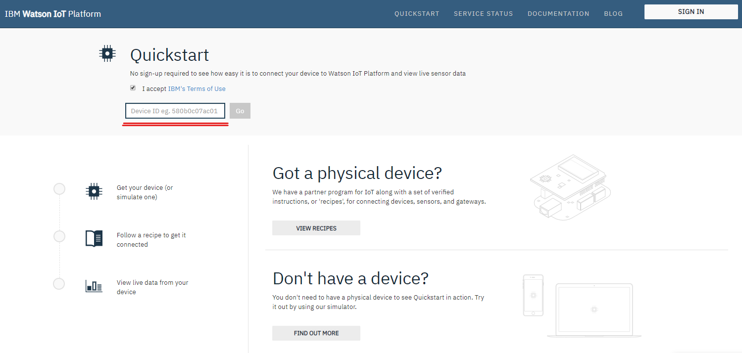
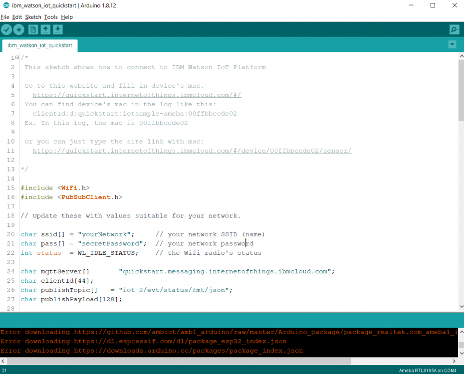
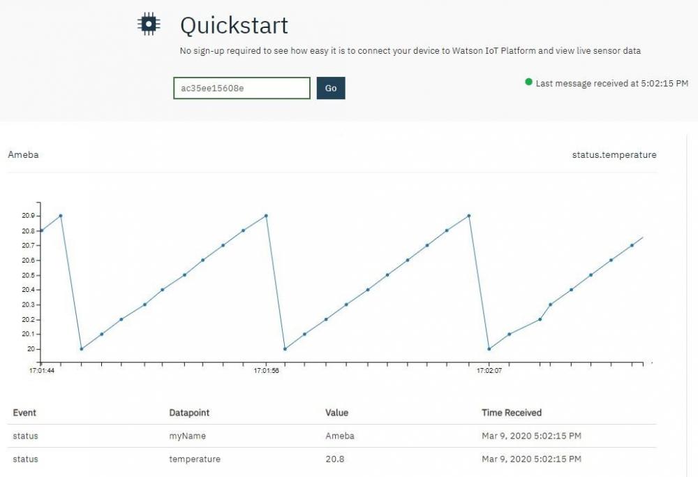
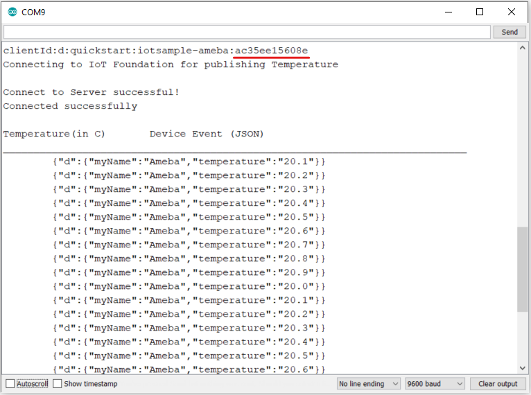
  4. MQTT (Message Queuing Telemetry Transport) is a protocol proposed by IBM and Eurotech. IBM® Watson™ IoT Platform is, by the official definition, “A foundational cloud offering that can connect and control IoT sensors, appliances, homes, and industries. Built on IBM Cloud, Watson IoT Platform provides an extensive set of built-in and add-on tools. Use these tools to process IoT data with real-time and historical analytics, extract key performance indicators (KPIs) from your data, add “smarts” in the cloud for non-smart products, and securely connect your own apps and existing tools to the Watson IoT Platform infrastructure.” (IBM, 2020) This platform provides easy web interface to register, connect and visualize our IOT devices. For quick start and simple try-out, registration is not necessary, we may just run our program to get the device ID needed for this platform. Preparation § Ameba x 1 Example In this example, we will take a look at how to make use of IBM Watson IOT platform for out IOT project. Open the MQTT example “File” -> “Examples” -> “AmebaMQTTClient” -> “ibm_watson_iot_quickstart” Make sure the Wi-Fi information is properly filled in and we are ready to upload the code to ameba. Once uploading finished, open a serial monitor and we shall see information as follows, Important: Please take note of the string of characters on the first line of the picture above -- “clientId:quickstart:iotsample-ameba:ac35ee15608e” “ac35ee15608e” is the device ID as well as the MAC address of the ameba board used here which will NOT be the same for other cases, so make sure to copy down the device ID displayed on your serial monitor. Next, we click the IBM IOT platform link provided here and open our browser: https://quickstart.internetofthings.ibmcloud.com/#/ Paste the device ID we just copied into the box highlighted below, If the device ID keyed in is correct, some fake temperature data that our ameba published will be visualized like this, Done! Now you have FREE and working IOT cloud platform to help you visualize your IOT data in realtime~
  5. Zero Multi-Power Supply (Battery supported) https://www.kickstarter.com/projects/349880250/zero-multi-power-supply-battery-supported
  6. Hello Everyone,We are pleased to announce the launch of our online store - Mynics.All of you are requested to check the website and do give us your valuable feedback.You can do the following at Mynics.in- Shop for electronics and robotics- Blogs- Forums- Projects and VideosWe are soon rolling out some great competitions and offers, do follow us to stay updatedhttps://www.facebook.com/mynics.in/http://stalkture.com/p/mynicsinsta/4934651665/https://plus.google.com/104613178419222567531Time to show your creativity and leave the rest to Mynics.Cheers,Team Mynics.
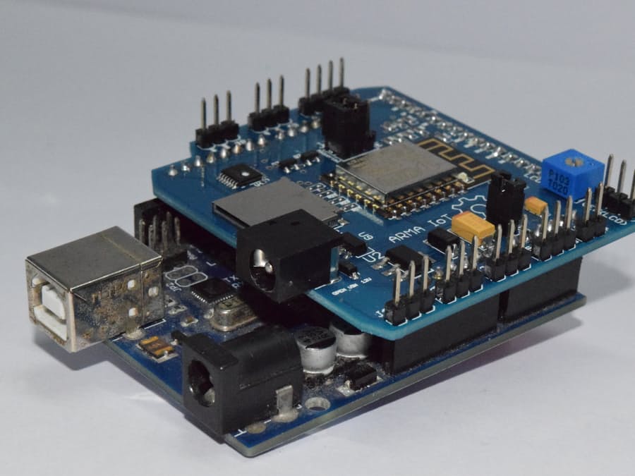
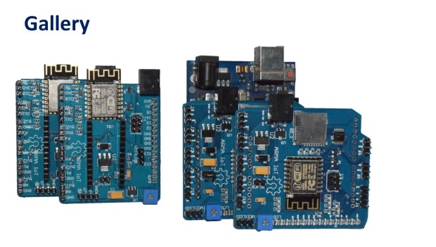
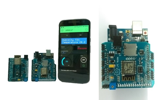
  7. Are u looking for a way to connect the Arduino to the internet easily? Do you want to develop your IoT project quickly without much hassle? ARMA IoT might just be the thing for you! The simple and efficient Arduino shield is powered through a esp12f wifi module, which enables it to be connected to the wifi network. it also has an SD card slot for for extra data storage like its wired brethren the Ethernet Shield. The ARMA IoT goes a step further and provides an easy plug and play feature for most of the common devices such as sensors, motors, LCDs and relays. The ARMA IoT is a great place for beginners to start their IoT project, as it requires minimum time to setup the hardware all thanks to the plug and play feature. Even the programming is simplified through the help of apps such as Blynk, which provides easy feature of controlling the Arduino through your Android or iOS phone. Thingspeak an upcoming IoT platform is also supported by the shield. The ARMA IoT platform proves as a tool for aspiring beginners and also a prototyping tool for advanced users. IoT products can be developed much faster with the help of this board. Weather it is creating a simple IoT project such as blinking LEDs or controlling relays, or developing your own Home automation system, the ARMA IoT facilitates it all and things seem to happen rather quickly with all the features provided on the board. The wifi connection feature can provide fast communication between devices or two instances of ARMA itself, making it applicable for simple swarm robotics, wireless controllers etc. The applications can also be extended to simple robotics, Energy management systems and it does not stop there as it all depends upon the users creativity. To get started simple tutorials are provided on the YouTube page of ARMA IoT, the link below guides on the setup of Arduino and ARMA IoT with the help of Blynk app More tutorials and projects will be posted to help you make the most of the shield. Of Course there are also various DIY communities that can provide you with both support and inspiration for your upcoming IoT projects. thus ARMA is another simple board that has the ability to bind many devices together. The ARMA IoT is still undergoing a crowdfunding campaign in Indiegogo and is available for pre-order. https://www.indiegogo.com/projects/arma-iot-breakout-board-for-arduino#/
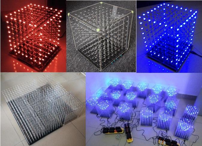
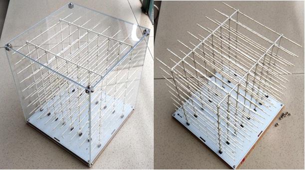
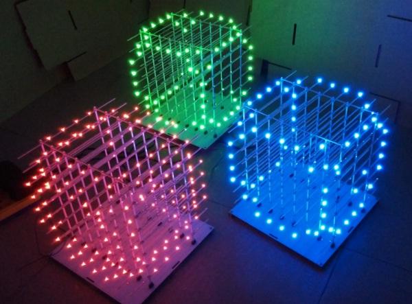
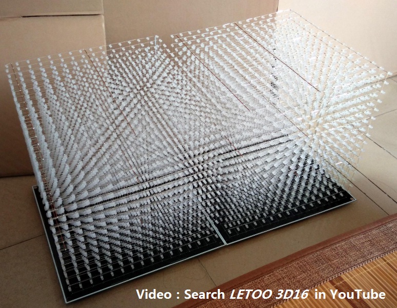
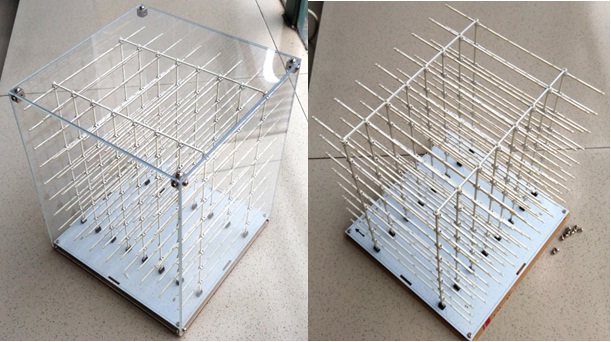
  8. Show you my DIY 3D 8×8×8 light cube.It’s reaaaally cool!
×
  • Create New...