Capacitor Substitution

davenn

Moderator
Sep 5, 2009
14,470
Joined
Sep 5, 2009
Messages
14,470
OK. There are pictures of the mosfets above. Is he asking for more than that? Forgive me if I sound like I'm an amateur, but I am. :)


this pic ?
converter-components-attached-to-heat-sink-right-side-jpg.46169


The case for those MOSFETs is a TO-247AC
 

WHONOES

May 20, 2017
1,242
Joined
May 20, 2017
Messages
1,242
Can you provide close up photo's (as close as you can whilst still in focus) on both sides of the board around the burnt area?
 

H2814D

Nov 4, 2017
258
Joined
Nov 4, 2017
Messages
258
Sure. Here you go. Note that although there was substantial heat there, the resistors are still measuring out correctly. The top portion of the board does not have any burn marks. The shroud on the mains does though. There are cotton fibers from a q-tip on some of the pointy solder bits in the bottom view.

The arcing that I mentioned above was visible directly in front of the middle post (Drain) of the mosfets (IRFP450) in the picture above through the board. There were no burn marks there either before or after seeing the arcing.
 

Attachments

  • Bottom of PCB Under Vertical Resistors.JPG
    Bottom of PCB Under Vertical Resistors.JPG
    113.4 KB · Views: 11
  • Vertical Resistors Front.JPG
    Vertical Resistors Front.JPG
    88.5 KB · Views: 10
  • Vertical Resistors Inside.JPG
    Vertical Resistors Inside.JPG
    77.1 KB · Views: 10
  • Vertical Resistors Rear.JPG
    Vertical Resistors Rear.JPG
    62.3 KB · Views: 9
Last edited:

H2814D

Nov 4, 2017
258
Joined
Nov 4, 2017
Messages
258
Sounds like you have a problem with a current limiting circuit cutting in to early. This could be due to a sense resistor getting a bit frazzled and its resistance increasing a bit or it might be the active element be it transistor or IC having a problem. I would check for a low value resistor that looks as though it has got very hot. An indication of this might be carbonisation of the PCB or the part itself or, it may even have created its own dry joint by getting hot enough to melt its solder joints.
Are you able to tell me if these are the "sense resistor(s)" you are talking about? They are low value (.1 Ohm) and are in parallel with each other. One end is in circuit contact with the number three leg (source) of both of the mosfets (IRFP450). You can see the connections in the photos attached to this reply.

Now if I was to replace these resistors, do I look for wire wound or current sense resistors? Are they the same thing as long as I get the correct values? They look like wire wound. They are 24mm long and 8mm diameter. I am guessing 5 watt?
 

Attachments

  • Better Pic of PCB Bottom.JPG
    Better Pic of PCB Bottom.JPG
    146.2 KB · Views: 7
  • .1 Ohm Resistor.JPG
    .1 Ohm Resistor.JPG
    35.4 KB · Views: 7
  • .1 Ohm Resistor Location on PCB.JPG
    .1 Ohm Resistor Location on PCB.JPG
    47 KB · Views: 8
  • PCB with .1 Ohm Resistors Removed.JPG
    PCB with .1 Ohm Resistors Removed.JPG
    52.9 KB · Views: 7

H2814D

Nov 4, 2017
258
Joined
Nov 4, 2017
Messages
258
OK all. I have to report a success here. Thanks for your help.

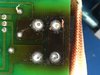
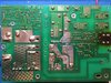
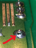
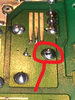
Today, since there weren't really that many of each, I decided to pull a leg off of all of the resistors, diodes, transistors, etc., and other easily testable components and do just that...test them. Everything tested ok, so I soldered each of the pulled legs/components back to the board. As I was re-soldering on the bottom of the board, I happened to glance at the top/inner leg of where "RT1" comes through the board from the other side. It is a thick coiled wire (Someone tell me what that (RT) is please? I tried but couldn't find "RT"). It was then that I noticed a cold solder joint that had not been there before. You can actually see that there is a difference between an earlier message pic of the bottom side of the PCB and the pic I have posted in this message.

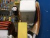
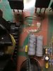
So I am confident that this is what happened: After removing the converter from the RV to begin my initial inspection I checked for visual signs of failure. This included cold solder joints and damaged/burned electronic components. Finding none, I decided to start testing individual components. In order to remove the heat sink from the PCB to get to the mosfets and the larger diodes attached to it, I had to remove the single vertical white resistor. It was in the way of a screw that holds a metal plate that holds the two mosfets and one of the thermal components to the heatsink. I had to take a long screwdriver and snake it between the RT1 and the two larger caps to get to the screw. The screw was tight and difficult to remove. I am sure I put pressure against the RT1 wire and that was what caused the solder joint to break. After testing the components, replacing everything, and powering back up- because I did not have any idea that I had caused the break- I am certain that that was what caused the flickering/arcing below the mosfets drain legs. As stated above, at that point I stopped and came back here for ideas. Because I had already inspected for broken solder joints, and found none, I assumed that wasn't the issue. Hindsight tells me I should have checked again. Amateur. :)

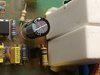
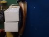
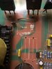
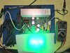
Anyway, today, after finding that break, reflowing the solder around it, and putting everything back together, I can happily say that I am getting 13.8vdc at the outputs, I can power a 12vdc LED fishing light without a substantial voltage loss, and am confident I have a working converter again. The original issue with the caps needing to being replaced and later finding the solder break, with your help, has saved me about $250USD!!! So thanks for that. And as a side note, hopefully someone else will come across this thread and get as lucky as I did.

I have attached pics of the break, the RT1 coiled wire, and a working converter powering a very bright LED fishing light (covered so it didn't wash out the photo).

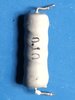
On a side note, those two vertical resistors standing right next to each other, were about 250F when measured with an infrared thermometer. They are 10W1K5J resistors. Can anyone advise if there would be a more suitable/cooler replacement for these? The heat they have produced, that actually marked the board, is my concern.

Thanks again, guys. I appreciate it.
 

Attachments

  • Cold Solder Joint Inner End of RT1.png
    Cold Solder Joint Inner End of RT1.png
    428.7 KB · Views: 13
  • Cold Solder Joint Farther Away View.png
    Cold Solder Joint Farther Away View.png
    510.6 KB · Views: 13
  • Functioning Power Converter Lightened.jpg
    Functioning Power Converter Lightened.jpg
    110.9 KB · Views: 12
  • Top of PCB- RT1- That Had Cold Solder Joint.png
    Top of PCB- RT1- That Had Cold Solder Joint.png
    368.4 KB · Views: 13

WHONOES

May 20, 2017
1,242
Joined
May 20, 2017
Messages
1,242
RT1 may be the current sense resistor which would make sense if you found that it had a dry joint and all is now working OK since you rectified it. Well done, glad you have got it sorted.
 
Top