Comparator inputs

KrisBlueNZ

Sadly passed away in 2015
Nov 28, 2011
8,393
Joined
Nov 28, 2011
Messages
8,393
You're welcome :) I enjoy helping, especially on projects that I find interesting.

I mentioned Skype because I think I will need to be involved during testing and debugging. As you said, this is not a trivial circuit, and getting it running properly will not be trivial. Communicating by posts is too inefficient. Skype is much better.

The circuit currently doesn't have a clearly defined behaviour when BOTH phase currents are above 32A. I think I'll have to add something to make sure it does. What behaviour would be appropriate?

I'm very glad you have an oscilloscope. I guess you have a multimeter too?

How do you plan on building the circuit? Do you have a breadboard?
 

Viad

Feb 9, 2012
29
Joined
Feb 9, 2012
Messages
29
I use Facetalk which is much the same thing I guess, it's a programme for a Mac . I can no doubt download something like Skype if Facetalk isn't compatible, I can look into that should the need arise.
I have a couple of small ancient Vero Breadboards I will use and finally make it up on Veroboard (stripboard)
Yes I have a multimeter, good old Avo 8, a digital one also but I prefer the Avo 8
I will think about the behaviour above 32A
many thanks
 

Viad

Feb 9, 2012
29
Joined
Feb 9, 2012
Messages
29
KrisBlue, I have built the circuit on a bread board. I have checked it several times and so I am fairly confident that it's correct.
As it stands so far the relay is energised and LED 1 is off
Before I go any further can you confirm that your connections for the current transformers is correct, having one side of the transformers common is ok ? as I seem to have similar waveforms at both U1A and U1B with only one CT connected. If you are sure the inputs are ok then I will spend more time on the circuit.
thanks
 

KrisBlueNZ

Sadly passed away in 2015
Nov 28, 2011
8,393
Joined
Nov 28, 2011
Messages
8,393
Yes, one side of each current transformer's secondary connects to the VAR rail, so they are connected together.

The VAR rail should measure about 2.8V DC relative to the 0V rail of the circuit. This should also be the DC voltage at pins 1 and 7 of the IC. Connect an oscilloscope to pins 1 and 7 of the IC and you should see the current waveforms, with a DC offset equal to VAR. The negative half-cycles of this waveform on pins 1 and 7 will be clipped if the waveform is large enough; this is normal.

I will be able to Skype from Tuesday around lunch time New Zealand time (GMT+13 at the moment). I'm awake at all hours but I don't normally have Skype running. Contact me by email or through Google Talk.
 

Viad

Feb 9, 2012
29
Joined
Feb 9, 2012
Messages
29
OK Kris, after correcting one wrong connection the voltages and waveform are as your description
But now I find that the inputs in effect common, whatever appears on pin 1 also appears on pin 7
Both pin 7 and 1 will rise together to the highest input on either of the inputs .
If it is of any help the resistance between pins 2 and 6 without the cts connected is 7k and with the cts connected is 200 ohm.
Could your circuit be at fault, or must I go and check my connections all over again.
thanks
 

KrisBlueNZ

Sadly passed away in 2015
Nov 28, 2011
8,393
Joined
Nov 28, 2011
Messages
8,393
Resistance between pins 2 and 6 with the CTs connected should be the sum of the secondary resistances of the two CTs. Assuming each CT has a 100 ohm secondary, 200 ohms would be right.

Pins 1 and 7 are the signals from the two CTs. If the CTs are connected in the same phase line, then pins 1 and 7 should have the same signal on them. If one of the CTs is not wired in, then only one of those pins should have a signal on it.

BTW sorry for my confusing suggestions about PMs and Skype. At this stage I would like discussion to stay on the forum; when you get to a point where this is wasting too much time and/or you are close to a working circuit, we can move to IM.

Unfortunately I blew out my monthly traffic allocation, so I won't be able to do voice/video chat until the 23rd of Feb! We can use Skype text chat or Google Talk though.
 

Viad

Feb 9, 2012
29
Joined
Feb 9, 2012
Messages
29
Hi KrisBlue, I have had problems with the input of your circuit, there is an interaction between the inputs . The outputs of the U1A and U12 both reach the same level despite the inputs T1 and T2 being at different levels. The output of both U1A and U1B both reach a level relative to the highest input.
I rebuilt the circuit with the same results.
I have rebuilt the first section of your circuit and have biased the op amps separately .
I have also made the output circuitry the same.
The first section is now behaving as it should but you could probably improve on my biasing circuit.
I have shown the voltages at the outputs A and B for different current levels at the CTs. Hope you can read the scan, you see something reaches it's limit at out put B, sitting at 5.1 V Pk to Pk despite increases in current.
Both charts show Pk Pk readings
The other chart shows voltages obtained from the CTs only using a burden resistor
two sizes 82 ohm and 180 ohm , this was something I had measured in my earlier attempts , but might be of interest to you .
In my earlier attempts at making this circuitry I used a burden resistor directly after the current transformer I then fed the ac output through a capacitor to block the biasing DC from the CT
I wonder which part of your circuit is behaving as a burden resistor, how is it calculated ?
I look forward to your reply
 

Attachments

  • Mod outputs.jpg
    Mod outputs.jpg
    143.9 KB · Views: 159

KrisBlueNZ

Sadly passed away in 2015
Nov 28, 2011
8,393
Joined
Nov 28, 2011
Messages
8,393
Oh ****! You're right. I'm really sorry!
Yes there will be interaction between the two inputs because of the current flowing in the current transformer, which will affect the bias rail.
I didn't think clearly about this when you described the problem. You're absolutely right. Please accept my apologies!

That circuit needs a bias rail with a very low impedance in order to work properly. I should have connected the shunt (burden) directly across the transformer rather than putting it in the feedback loop (RC1 and RC2 are the shunt resistors). I know that's the traditional way but I thought that my design was being clever. Now I can see that it casues major problems.

I will post a corrected circuit soon. Again please accept my apology for wasting your time.
 

KrisBlueNZ

Sadly passed away in 2015
Nov 28, 2011
8,393
Joined
Nov 28, 2011
Messages
8,393
attachment.php


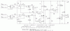
Here's a corrected version. I've connected the shunt straight across the transformer in the usual way, and used a voltage follower stage as a buffer for each transformer. You might be able to get away without the buffer stage at all, with a few component value changes later in the design, but you have a quad op-amp so you might as well use it.

This change also means that a special high-current op-amp IC isn't needed.

Again I apologise profusely for wasting your time with a flawed design. I should have been able to see the error as soon as you described the problem.
 

Attachments

  • VIAD.002.GIF
    VIAD.002.GIF
    16 KB · Views: 183

Viad

Feb 9, 2012
29
Joined
Feb 9, 2012
Messages
29
Hi KrisBlue, no need for apologies, your second circuit works thanks . I think though I am going to have to start from scratch. I never realised there would be so many variables to sort out and it's getting to be a slog now, particularly as I am lacking in knowledge of the circuits. It doesn't help that it;s all on a bread board where components or connecting links have a habit of disconnecting. IC pin 9 reaches a max of 5.3V at a CT current of 30A plus and pin 12 sits at 8V doesn't seem to want to switch QR on even if volts on other pin exceeds it .
What advantage are the two buffers ?
Can this circuit be simplified ?
Thanks for your help so far
 

KrisBlueNZ

Sadly passed away in 2015
Nov 28, 2011
8,393
Joined
Nov 28, 2011
Messages
8,393
The only simplification I can see would be to remove the two input buffers, but that would necessitate a "firmer" VAR rail. The saving, if any, is not significant. I don't see any way to simplify the rest of the circuit. Actually it's a pretty compact design I think.

Does the LED correctly indicate which CT has the higher current? Can you check that pins 9 and 10 increase when the relevant CT current increases and decreases when it decreases?

I can help via Skype, but not until the 23rd (I've used up my monthly data allocation so I'm limited to 64kbps until it renews).
 

Viad

Feb 9, 2012
29
Joined
Feb 9, 2012
Messages
29
Kris, yes the LED lights, perhaps I've knackered U1D pin 14 won't change whatever I do to the inputs.
By the way pin 12 sits at 8V
Can you explain what you mean by a 'firmer' VAR rail and why ?
thanks
 

KrisBlueNZ

Sadly passed away in 2015
Nov 28, 2011
8,393
Joined
Nov 28, 2011
Messages
8,393
The input to the final comparator is on pin 13 not pin 12. The voltage on pin 13 should follow the LED state but with a delay due to CD being charged and discharged through RD. When the LED is ON, the pin 13 voltage should increase towards 12V (it will never quite reach it though; don't worry about that) and with the LED OFF, the pin 13 voltage should decrease towards 0V (it will never quite reach it either). Does that happen?

Re the VAR rail. At present it's just a voltage divider with a decoupling capacitor. This produces the desired voltage, but only if no current flows into the rail. That was the problem with my initial design - the current that was flowing in the current transformers was feeding into the VAR rail and causing the VAR voltage to change, which coupled into the other input and caused the problems you found.

You could say that the problem happened because the VAR rail was not "firm" enough - its voltage did not hold steady as current was drawn from, or fed into, the rail. There are ways to generate a firm rail using a little IC called a "rail splitter", but if the circuit can be changed so that it doesn't feed any current into the VAR rail, or draw any current out of the VAR rail, then the simple two-resistor divider is fine.

With the circuit the way it is now, no current flows into the VAR rail, so it stays nice and stable, and the circuit works as intended.

You can remove the buffer stages. To do this, delete RS1 and U1A, and connect the top end of T1 secondary straight to RD1. Do the same thing for the second channel.

The problem here is that RD1 requires some current every time the peak CT current increases above the value stored in CT1. This current flows through RD1 and DR1, and charges CT1. This current will also flow into the VAR rail and cause the VAR voltage to change, which will affect the other channel.

This problem can be reduced by making the VAR rail "firmer", by reducing RH1 and RH2 (keeping their values in proportion), for example using 330 ohms and 100 ohms. This increases the circuit's current consumption though.

Alternatively you can use a rail splitter to provide the VAR rail voltage. There's a device called a TLE2425 from Texas Instruments that will do this. This produces a 2.5V rail that is very firm and will not be affected by the CT1 and CT2 charge currents.

But since you already have a quad op-amp I think the simplest approach is to keep the buffers. In other circumstances I might suggest using a TLE2425 and omitting the buffers, and using a dual op-amp instead of a quad. I like and recommend the MC34072 for general dual op-amp applications.
 

EinarA

Feb 11, 2013
28
Joined
Feb 11, 2013
Messages
28
Viad is probably to far along to want to change but there is simpler way if the voltages from the transformers are big enough drive the rectifiers directly. By converting one signal to a positive voltage and the other to a negative one when you combine them through equal valued resistors the result will be easy for the comparator: when input one is higher the voltage will be positive and when input two is higher the voltage will be negative. The second section provides delayed drive for a relay.
I meant to show the unmarked diodes as schotky or Ge types. The 1M R at the neg input to sec A would be better as 330K.
 

Attachments

  • image.jpg
    image.jpg
    79.1 KB · Views: 166
Last edited:

KrisBlueNZ

Sadly passed away in 2015
Nov 28, 2011
8,393
Joined
Nov 28, 2011
Messages
8,393
EinarA, Duke37 suggested that in post #5 on this thread. Actually his solution was slightly simpler - rectify the two CT outputs and simply connect them in series with opposing polarities. At least that's what I think he meant.

The problem I have with that approach is the deadband near the bottom of the range where the voltage from the CT is less than the diode's forward voltage. But that could be eliminated with biasing, without complicating the design too much. I also wanted to have hysteresis, but that could be added to your design as well.

Edit: Doh! You did include hysteresis. The hysteresis you've implemented around the final comparator doesn't look right to me. What are the upper and lower trigger voltages you're aiming for, EinarA?

BTW you should get LTSpice from http://www.linear.com. Even if you don't use the simulation features, it will produce nice-looking schematics, and it's free!
 
Last edited:

duke37

Jan 9, 2011
5,364
Joined
Jan 9, 2011
Messages
5,364
The basic idea as Kris says was to rectify the two signals and subtract one from the other.
If the bridge rectifier is placed between the transformer and the resistor, then the effect of the diode voltage drops will be minimised since the output impedance of the transformer will be hgjh.
 

KrisBlueNZ

Sadly passed away in 2015
Nov 28, 2011
8,393
Joined
Nov 28, 2011
Messages
8,393
If the bridge rectifier is placed between the transformer and the resistor, then the effect of the diode voltage drops will be minimised since the output impedance of the transformer will be hgjh.
Doh! Why didn't I think of that.
 

EinarA

Feb 11, 2013
28
Joined
Feb 11, 2013
Messages
28
Duke's first posts did remind me to connect them this way. I also considered putting the diodes as he suggests above, but left it off the schematic. The circuit does have hyteresis, its R6 ( I think , I can't read it from here.). The circuit can be configured to switch when input one is slightly above input 2 and back when it they are nearly equal. Or it can switch to whichever is larger and stay with that until the other one is larger. I tried LTSpice but found it too tedious; perhaps it is easier on an iPad.
Reading your editted post; the switch points for sec A are about .12V and .06V ( mostly guesses as to suitibility ). For sec B they are 1.5V and about 8V. The connection is non-standard but reduces resistors.
 

KrisBlueNZ

Sadly passed away in 2015
Nov 28, 2011
8,393
Joined
Nov 28, 2011
Messages
8,393
OK, I've taken duke37's suggestions and drawn up a new circuit.

Even if Viad doesn't want to change his circuit, I'm interested in coming up with the best design possible.

I've had no experience with current transformers so I'm just learning the techniques. I see this as a learning exercise for me, mainly!

I'm keen to hear opinions from duke37 and EinarA, and anyone else who has used current transformers before.

attachment.php


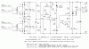
I've used full-wave rectification, with the shunt after the diodes, and the two signals connected in series with opposite polarity, as duke37 suggested.

Full-wave rectification has the advantage that the polarity of the CTs doesn't have to be maintained.

CS1 and CS2 provide a small amount of smoothing but are mainly there to reject high-frequency interference. (Xc of 0.22 uF at 120 Hz is about 6k.) So these signals will be full-wave rectified but unsmoothed.

The sum of the two opposing signals is filtered by RF and CF (330k and 1 uF) which has a time constant of 0.33 seconds, which is 33 or 40 half-cycles (50 or 60 Hz mains).

This voltage is offset to a half-supply-voltage rail and fed into a comparator with adjustable hysteresis, and an adjustable nominal threshold to allow the choice to be biased in favour of one or other CT. The output is delayed by RD and CD (T=33 seconds) and fed to the final comparator which drives the relay.

For the final comparator I've used EinarA's nifty trick of splitting the output voltage to provide the positive feedback instead of using a three-resistor network on the non-inverting input, which saves one or two resistors. I changed the resistor values to set the trigger points at 1/3 and 2/3 of the supply voltage, which is needed to give equal time delays in each direction of the decision. I'll remember this little trick!

Since no op-amps are needed, I've switched to an LM393 dual comparator.

Opinions or further suggestions, anyone?
 

Attachments

  • VIAD.003.GIF
    VIAD.003.GIF
    13.7 KB · Views: 226

duke37

Jan 9, 2011
5,364
Joined
Jan 9, 2011
Messages
5,364
Kris,

I am no expert on current transformers.

The circuit looks pretty good to me, the only thing I would question is that the hysteresis control is linked to the set point. Thus there will some interaction.
Would it be better to put a variable resistor across the comparator.

Duke37
 
Top