transistor sizing for AND gate?

vead

Nov 27, 2011
473
Joined
Nov 27, 2011
Messages
473
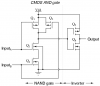
AND gate with cmos transistor
we can create cmos AND gate with 3 nmos and 3 pmos transistor

pmos 1 and pmos 2 connected in parallel

nmos 1 and nmos 2 connected in series

nmos 3 and pmos 3 connected in series for inverter circuit

inverter with nmos 3 W/L=3/2 and pmos 3 W/L=6/2

parallel pmos (L will double with same W)

pmos 1 W/L=6/4 and pmos 2 W/L = 6/4

nmos series ( W will double with same L)

nmos 1 W/L= 3/4 and nmos 2 W/L=3/4


nmos 1 W/L=6/4
nmos 2 W/L=6/4
nmos 3 W/L=3/2


pmos 1 W/L=3/4
pmos 2 W/L=3/4
pmos 3 W/L=3/2

IS this correct sizing for AND gate
 

Harald Kapp

Moderator
Moderator
Nov 17, 2011
14,271
Joined
Nov 17, 2011
Messages
14,271
1) An image says more than thousan words. It is not easy from your verbal description to get an idea how your circuit looks like. Show us a schematic, please.
2) as a rough approximation an NMOS transistors conductivity in the ON state is roughly 2* that of a PMOS transistor (assuming same W/L). Therefore you make W/L(pmos)=2*W/L(nmos) for approximately equal ON resistance.

The numbers in your post are inconsistent :
inverter with nmos 3 W/L=3/2 and pmos 3 W/L=6/2
versus
nmos 3 W/L=3/2 and pmos 3 W/L=3/2 in the tabular isting at the end.

Clear up your numbers, draw a schematic and come back.

Here's some reading material.
 

vead

Nov 27, 2011
473
Joined
Nov 27, 2011
Messages
473
pmos 1 and pmos 2 connected in parallel

nmos 1 and nmos 2 connected in series

nmos 1 W/L=6/4
nmos 2 W/L=6/4
nmos 3 W/L=3/2


pmos 1 W/L=3/4
pmos 2 W/L=3/4
pmos 3 W/L=3/2
 

Attachments

  • 04146.png
    04146.png
    7.1 KB · Views: 494

Harald Kapp

Moderator
Moderator
Nov 17, 2011
14,271
Joined
Nov 17, 2011
Messages
14,271
I can guess what you mean, but you're making it difficult to follow your reasoning. The transistors in the schematic have different numbers than those you quote in your post.

What is the reason NMOS 1 and 2 have 2*W/L of PMOS 1 and 2 but NMOS 3 and PMOS 3 have the same W/L? Consider the reasons why you have chosen W/L for NMOS/PMOS 1 and 2 in that way and re-read my first answer to find a reasonable W/L for NMOS3 and PMOS 3.
 

vead

Nov 27, 2011
473
Joined
Nov 27, 2011
Messages
473
Q1 nmos W/L=6/4
Q2 nmos W/L=6/4
Q5 nmos W/L=3/2

Q3 pmos 1 W/L=3/4
Q4 pmos 2 W/L=3/4
Q6 pmos 3 W/L=3/1


given, Q5 nmos W/L=3/2
Q6 pmos 3 W/L=3/1
Q I want to determine size Q1,Q2,Q3 ,Q4

I want to size transistors so that output resistance is same as inverter
 

Harald Kapp

Moderator
Moderator
Nov 17, 2011
14,271
Joined
Nov 17, 2011
Messages
14,271
1) 6/4 = 3/2
2) You have W/L(pmos) = 1/2*W/L(nmos). Go back and read my 1st answer.
 

vead

Nov 27, 2011
473
Joined
Nov 27, 2011
Messages
473
I tried but I didn't understand how to do transistor sizing give me sample example

1)can we keep same size ?
2) when we size transistor what should we know?
 

Harald Kapp

Moderator
Moderator
Nov 17, 2011
14,271
Joined
Nov 17, 2011
Messages
14,271
You need to understand the importance of W/L. Why is W/L an important parameter for a MOSEFT? Hint: look at the equations for Ids.

In your first post you state
inverter with nmos 3 W/L=3/2 and pmos 3 W/L=6/2
That is correct, but do you know why? Compare the ON resistance of an NMOS and a PMOS with same W/L ratio (it doesn't matter what the exact value of the ratio is. Or compare IDS(nmos) vs. IDs(pmos) which is a bit easier to do because the equations in teh link I gave you are for Ids, not for ON resistance.

Take IDS(nmos)/IDS(pmos), use the linear region, assume most parameters are the same (W, L, lambda, Cox, VT etc.). Note that the mobility µ(n) is approx. 2*µ(p). The ratio IDS(nmos)/IDS(pmos) will become a single number which tells you a lot about the difference between NMOS and PMOS transistors.

Once you have done this and have understood the difference, use the same equation IDS(nmos)/IDS(pmos), but use W(n)/L(n) and W(p)/L(p) to allow for different geometries of the NMOS and PMOS transistors. To simplify the equation, set W(n)/L(n)=X, W(p)L(p)=Y. You will then have an equation with the parameters X, Y, µ(n), µ(p). Again setting µ(n)=s*µ(p) (Note: only an approximation!), what is required for the ratio X/Y to arrive at IDS(nmos)/IDS(pmos)=1, that is both NMOS and PMOS are equally good conductors in the ON state?

You will now see why the ratio W/L is important, not the absolute values for W and L. With that knowledge in hand, consider:
  • What happens to the ON resistance (or Ids) when two NMOS transistors are in series (i.e. both inputs of the AND gate are high)?
  • Why do you have to take into account only one PMOS transistor when considering on low input of the AND gate?
  • Why is it required that the NMOS and PMOS transistors at the inverter (output circuit) have different W/L ratios?
 

vead

Nov 27, 2011
473
Joined
Nov 27, 2011
Messages
473
Its great help
ok now I can size Inverter but how to size big circuit like AND gate ,OR gate

how to think for big circuit ?
 

Harald Kapp

Moderator
Moderator
Nov 17, 2011
14,271
Joined
Nov 17, 2011
Messages
14,271
Consider transistors is series as e.g. the two NMOS in an NAND gate (or AND gate before the inverter). In order for a low output, both transistors have to be ON, their "resistances" add as in a series connection of resistors. The two PMOS in a NAND gate are in parallel. However, fo a high output only one has to be active.
Now think of the "resistances" of the two seroes conencted NMOS transistors versus the one PMOS. If you want to have approx. equal ON resistances for the High and the Low state, how do you need to schale W/L for the NMOS and the PMOS?
Start from the inverter, whci you say you now understand and simply add a second NMOS in the Low-path of the inverter. How do you have to scale W/L of the NMOS transistors to arrive at the same on resistance as with a single transistor?
 

vead

Nov 27, 2011
473
Joined
Nov 27, 2011
Messages
473
ok

Nmos W/L=3/2 and Pmos W/L=6/4( transistor in inverter circuit)

caseI - when to mosfet in series this is similar to one transistor with double length and same width
Example two series nmos with W=1 and L=1
resultant W/L=1/2

case II when to mosfet in parallel W will be double with same L
Example- two pmos in parallel with w=1 and L=1
resultant W/L=2/1

So I made following sizing for AND gate circuit
nmos W/L=3/2 and pmos W/L=6/4 (inverter circuit)
nmos W/L=3/1 and pmos W/L=3/4 (for nand gate circuit)
 
Last edited:

Harald Kapp

Moderator
Moderator
Nov 17, 2011
14,271
Joined
Nov 17, 2011
Messages
14,271
Case I: o.k.
Case II: in principle o.k, but not fully.

Case I: o.k., because the two NMOS have to be both ON for a low output of the gate.
Case II: only partly o.k. because you are right, if both PMOS are ON, then you have effectively doubled the width. But for the output of the NAND to go high it suffices that one input is low. Therefore only one PMOS is active in the worst case (worst case as seen from the output's current driving capability). I tried to convey that idea in my previous posts, hopefully this statement makes it clear now.

nmos W/L=3/1 and pmos W/L=3/4 (for nand gate circuit)
With that design 2*NMOS in series have an effective W/L=3/2.
According to the above explanation the 1*PMOS needs to have the same conductivity as 2*NMOS. WIth W/L(pmos)=3/4 the conductivity of the PMOS is much less than that of 2*NMOS in series.
Go back and read my post #8. It seems that you haven't understood it. Do the math as explained there. Note especially the difference in electron mobility (µn) and hole mobility (µp). Assume µn=2*µp (a rough approximation only). Then design W/L(pmos) such that it leads to the same conductivity as 2*W/L(nmos)=3/2.
 
Top