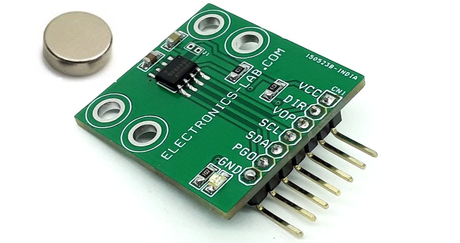
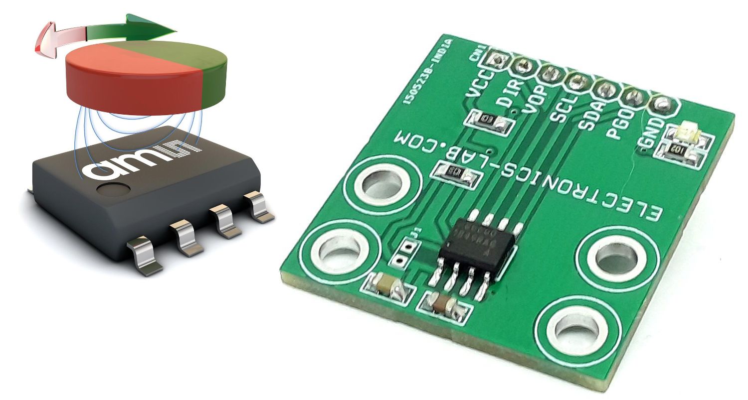
Contactless Potentiometer – 12bit Rotary Position Sensor with Analog or PWM Output
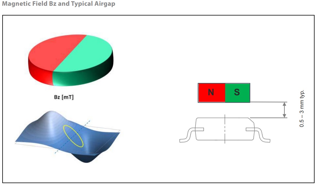
This is an easy-to-program magnetic rotary position sensor with high-resolution 12-bit analog or PWM output. This contactless system measures the absolute angle of a diametric magnetized on-axis magnet.

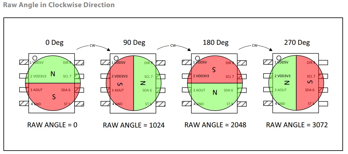
This is an easy-to-program magnetic rotary position sensor with high-resolution 12-bit analog or PWM output. This contactless system measures the absolute angle of a diametric magnetized on-axis magnet. The project is designed for contactless potentiometer applications and its robust design eliminates the influence of any homogenous external stray magnetic fields. The industry-standard I²C interface supports simple user programming of non-volatile parameters without requiring a dedicated programmer. By default, the output represents a range from 0 to 360 degrees. It is also possible to define a smaller range to the output by programming a zero angle (start position) and a maximum angle (stop position). The AS5600 is also equipped with a smart low-power mode feature to automatically reduce power consumption. An input pin (DIR) selects the polarity of the output with regard to rotation direction. If DIR is connected to the ground, the output value increases with clockwise rotation. If DIR is connected to VDD, the output value increases with counterclockwise rotation.
Applications
The AS5600 Module is ideally suited for contactless potentiometers, contactless knobs, pedals, RC servos, and other angular position measurement solutions.
- Standalone Operation: The module provides approx. 0 to 5V output with 0 to 360 degrees Magnet movement in standalone mode. Please refer to the datasheet of the ASM5600 chip for PWM output and programming.
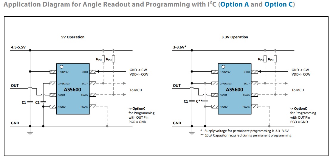
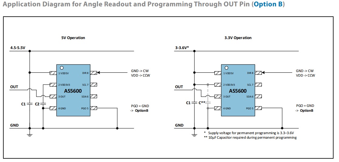
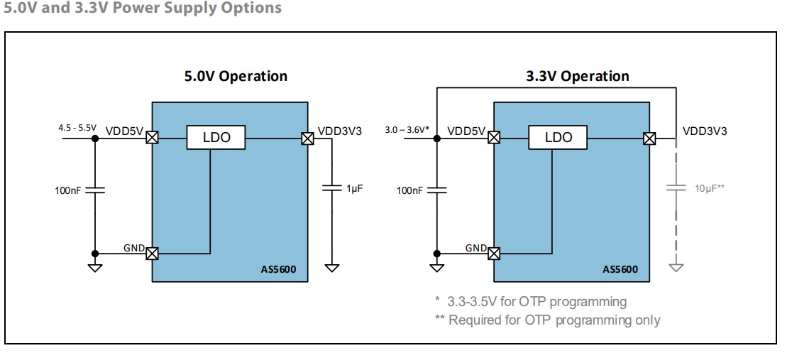
- Power Management: The module may be powered from a 5.0V supply using the on-chip LDO regulator, or it can be powered directly from a 3.3V supply. In 3.3V operation, the VDD5V and VDD3V3 pins must be tied together with onboard PCB solder jumper J1. VDD is the voltage level present at the VDD5V pin.
- Direction (clockwise vs. counterclockwise): The AS5600 allows controlling the direction of the magnet rotation with the DIR pin. If DIR is connected to GND (DIR = 0) a clockwise rotation viewed from the top will generate an increment of the calculated angle. If the DIR pin is connected to VDD (DIR = 1) an increment of the calculated angle will happen with counterclockwise rotation.
Features
- Supply 5V DC or 3.3V DC
- Output 12Bit Analog or PWM Output
- Default Output 0 to 5V with 0 to 360 degrees Magnet movement
- Sensing Range 0 to 360 degrees
- Simple user-programmable start and stop positions over the I²C interface
- Maximum angle programmable from 18° up to 360°
- 12-bit DAC output resolution
- Analog output ratiometric to VDD or PWM-encoded digital output
- I2C Interface for Easy Programming
- Output Polarity Selection Using Dir Pin, By pulling down or Pulling Up
- Automatic magnet detection
- 4 x 3.3MM Mounting Holes
- PCB Dimensions 29.21 x 27.31 mm
Analog Output Mode
By default, the AS5600 output stage is configured as an analog ratiometric output. The Digital to Analog Converter (DAC) has 12-bit resolution. In default mode, the lower reference voltage for the DAC is GND, while the upper reference voltage is VDD. The output voltage on the OUT pin is ratiometric between GND and VDD. The maximum angular range can be programmed from 18 degrees to 360 degrees. The default range is 360 degrees. As shown below, if the range is 360 degrees, to avoid discontinuity points exactly at the limit of the range, a 10-LSB hysteresis is applied. This hysteresis suppresses toggling the OUT pin when the magnet is close to zero or 360 degrees.
PWM Output Mode
The AS5600 output stage can be programmed in the OUTS bits of the CONF register for a PWM-encoded digital output (OUTS = 10). In this mode, the OUT pin provides a digital PWM signal. The duty cycle of each pulse is proportional to the absolute angle of the rotating magnet. The PWM signal consists of a frame of 4351 PWM clock periods as shown in Figure 30. This PWM frame is composed of the following sections: • 128 PWM clock periods high • 4095 PWM clock periods data • 128 PWM clock periods low The angle is represented in the data part of the frame, and one PWM clock period represents one 4096th of the full angular range. The PWM frequency is programmed with the PWMF bits in the CONF register.
I²C Interface
The AS5600 Module supports the 2-wire Fast-mode Plus I²C-slave protocol in device mode, in compliance with the NXP Semiconductors (formerly Philips Semiconductors) specification UM10204. A device that sends data onto the bus is a transmitter and a device receiving data is a receiver. The device that controls the message is called a master. The devices that are controlled by the master are called slaves. A master device generates the serial clock (SCL), controls the bus access, and generates the START and STOP conditions that control the bus. The AS5600 always operates as a slave on the I²C bus. Connections to the bus are made through the open-drain I/O lines SDA and the input SCL. Clock stretching is not included. The host MCU (master) initiates data transfers. The 7-bit slave address of the AS5600 is 0x36 (0110110 in binary). Supported Modes • Random/Sequential read • Byte/Page write • Automatic increment (ANGLE register) • Standard-mode • Fast-mode • Fast–mode plus The SDA signal is the bidirectional data line. The SCL signal is the clock generated by the I²C bus master to synchronize sampling data from SDA. The maximum SCL frequency is 1 MHz. Data is sampled on the rising edge of SCL.
I²C Modes
Invalid Addresses There are two addresses used to access an AS5600 register. The first is the slave address used to select the AS5600. All I²C bus transactions include a slave address. The slave address of the AS5600 is 0x36 (0110110 in binary) The second address is a word address sent in the first byte transferred in a write transaction. The word address selects a register on the AS5600. The word address is loaded into the address pointer on the AS5600. During subsequent read transactions and subsequent bytes in the write transaction, the address pointer provides the address of the selected register. The address pointer is incremented after each byte is transferred, except for certain read transactions to special registers. If the user sets the address pointer to an invalid word address, the address byte is not acknowledged (the A bit is high). Nevertheless, a read or write cycle is possible. The address pointer is increased after each byte. Reading When reading from an invalid address, the AS5600 returns all zeros in the data bytes. The address pointer is incremented after each byte. Sequential reads over the whole address range are possible including address overflow. Automatic Increment of the Address Pointer for ANGLE, RAW ANGLE and MAGNITUDE Registers These are special registers which suppress the automatic increment of the address pointer on reads, so a re-read of these registers requires no I²C write command to reload the address pointer. This special treatment of the pointer is effective only if the address pointer is set to the high byte of the register. Writing A write to an invalid address is not acknowledged by the AS5600, although the address pointer is incremented. When the address pointer points to a valid address again, a successful write accessed is acknowledged. Page writes over the whole address range is possible including address overflow. Supported Bus Protocol Data transfer may be initiated only when the bus is not busy. During data transfer, the data line must remain stable whenever SCL is high. Changes in the data line while SCL is high are interpreted as START or STOP conditions.
Accordingly, the following bus conditions have been defined: Bus Not Busy Both SDA and SCL remain high. Start Data Transfer A change in the state of SDA from high to low while SCL is high defines the START condition. Stop Data Transfer A change in the state of SDA from low to high while SCL is high defines the STOP condition. Data Valid The state of the data line represents valid data when, after a START condition, SDA is stable for the duration of the high phase of SCL. The data on SDA must be changed during the low phase of SCL. There is one clock period per bit of data. Each I²C bus transaction is initiated with a START condition and terminated with a STOP condition. The number of data bytes transferred between START and STOP conditions is not limited, and is determined by the I²C bus master. The information is transferred byte-wise and each receiver acknowledges with a ninth bit. Acknowledge Each I²C slave device, when addressed, is obliged to generate an acknowledge after the reception of each byte. The I²C bus master device must generate an extra clock period for this acknowledge bit. A slave that acknowledges must pull down SDA during the acknowledge clock period in such a way that SDA is stable low during the high phase of the acknowledge clock period. Of course, setup and hold times must be taken into account. A master must signal an end of a read transaction by not generating an acknowledge bit on the last byte that has been clocked out of the slave. In this case, the slave must leave SDA high to enable the master to generate the STOP condition.
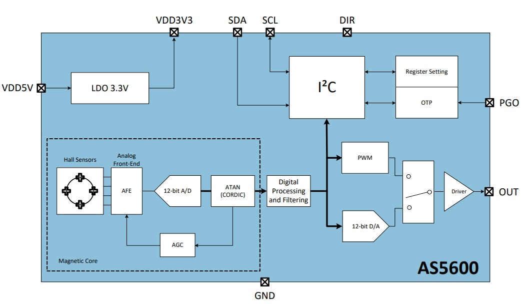
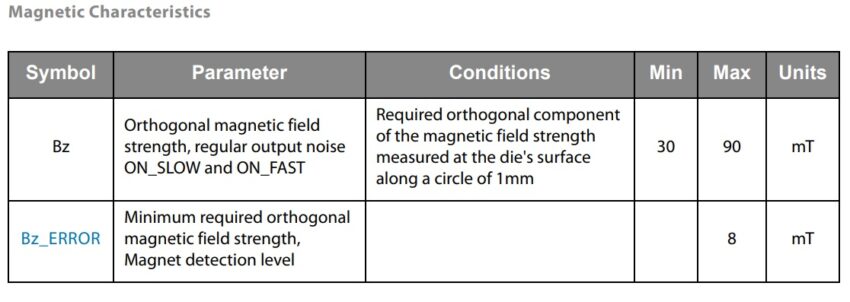
The AS5600 is a Hall-based rotary magnetic position sensor using planar sensors that convert the magnetic field component perpendicular to the surface of the chip into a voltage. The signals coming from the Hall sensors are first amplified and filtered before being converted by the analog-to-digital converter (ADC). The output of the ADC is processed by the hardwired CORDIC block (Coordinate Rotation Digital Computer) to compute the angle and magnitude of the magnetic field vector. The intensity of the magnetic field is used by the automatic gain control (AGC) to adjust the amplification level to compensate for temperature and magnetic field variations. The angle value provided by the CORDIC algorithm is used by the output stage. The user can choose between an analog output and a PWM-encoded digital output. The former provides an output voltage that represents the angle as a ratiometric linear absolute value. The latter provides a digital output which represents the angle as the pulse width. The AS5600 is programmed through an industry-standard I²C interface to write an on-chip non-volatile memory. This interface can be used to program a zero angle (start position) and a maximum angle (stop position) which maps the full resolution of the output to a subset of the entire 0 to 360 degrees range.
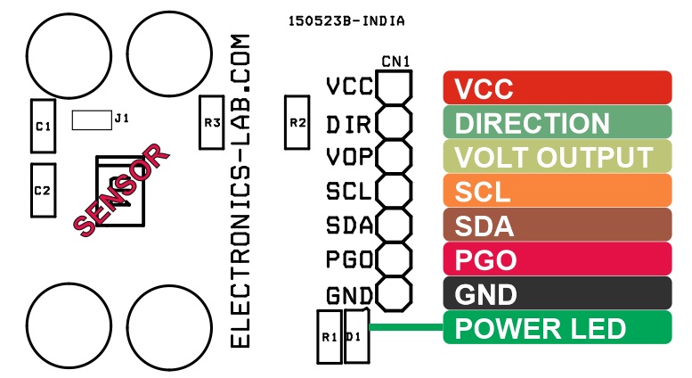
Connections
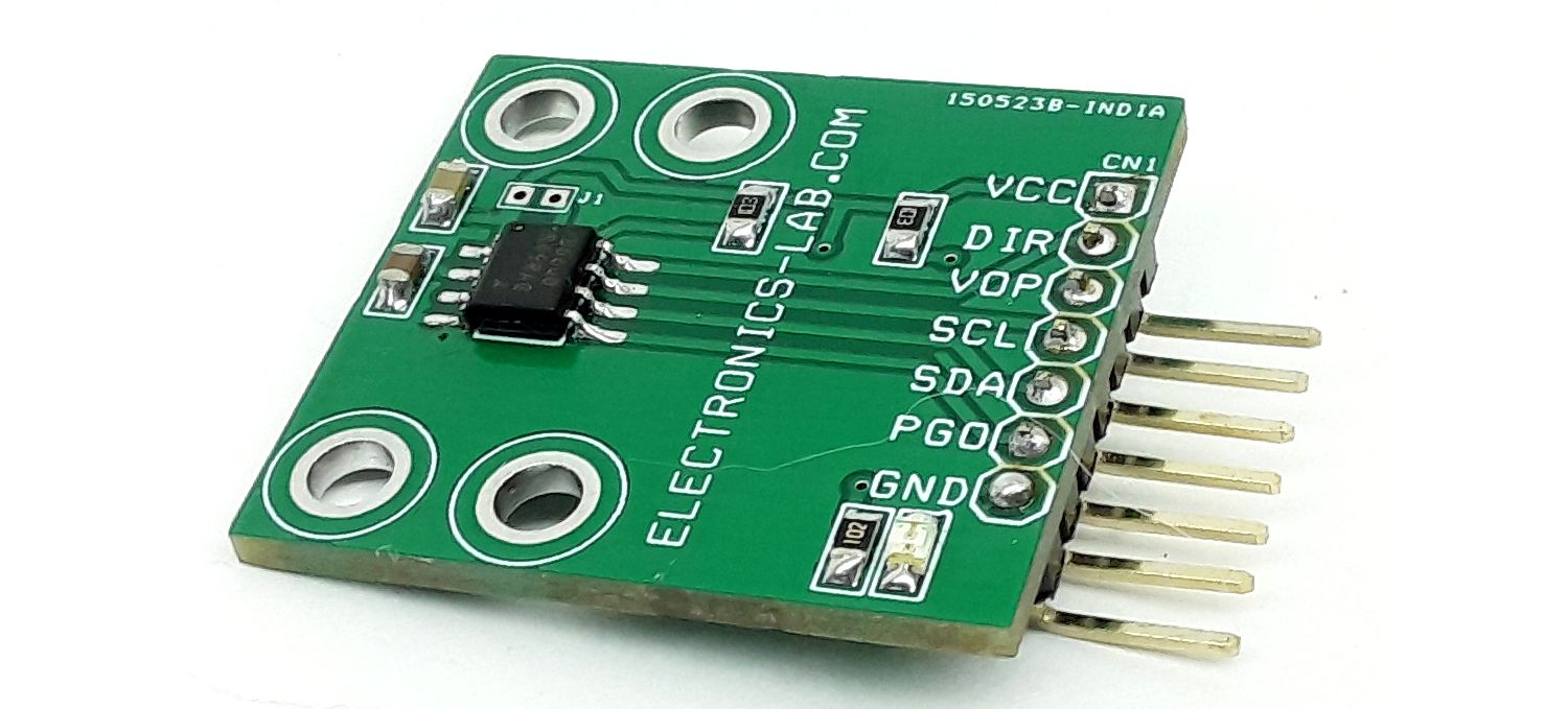
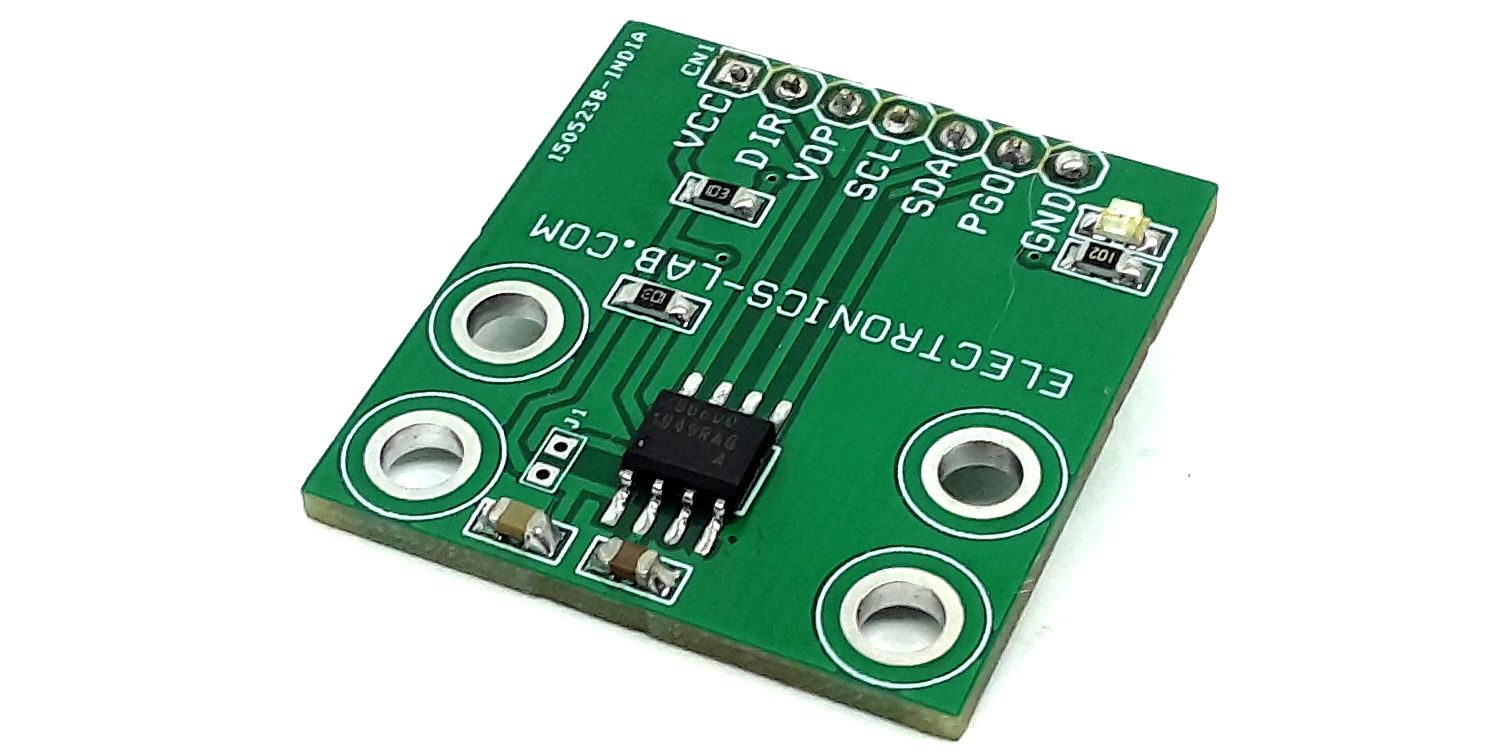
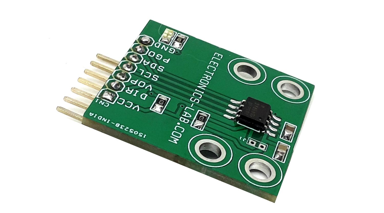
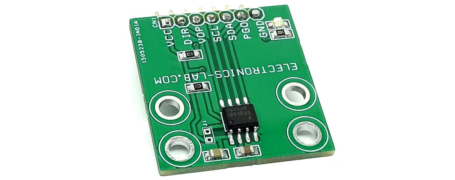
- CN1: Pin 1 = VCC 5V/3.3V, Pin 2 = Direction, Pin 3 = Voltage Output, Pin 4 = SCL, Pin 5 = SDA, Pin 6 = PGO, Pin 7 = GND
- D1 Power LED
- Jumper J1: PCB Solder Jumper, Solder for 3.3V Input
Schematic
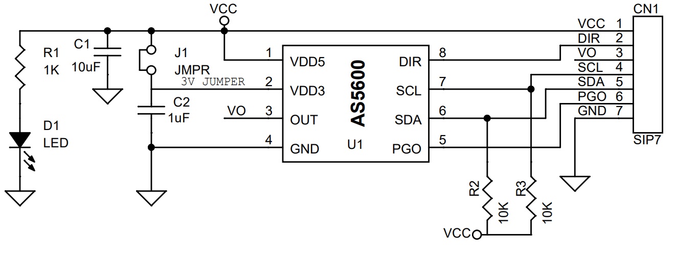
Parts List
| NO. | QNTY. | REF. | DESC. | MANUFACTURER | SUPPLIER | SUPPLIER'S PART NO |
|---|---|---|---|---|---|---|
| 1 | 1 | CN1 | 7 PIN MALE HEDAER PITCH 2.54MM | WURTH | DIGIKEY | 732-5320-ND |
| 2 | 1 | C1 | 10uF/10V CERAMIC SMD SIZE 0805 | YAGEO/MURATA | DIGIKEY | |
| 3 | 1 | C2 | 1uF/10V SMD SIZE 0805 | YAGEO/MURATA | DIGIKEY | |
| 4 | 1 | D1 | LED RED SMD SIZE 0805 | OSRAM | DIGIKEY | 475-1278-1-ND |
| 5 | 1 | J1 | JUMPER PCB-SOLDER | SOLDER JUMPER | ||
| 6 | 1 | R1 | 1K 5% SMD SIZE 0805 | YAGEO/MURATA | DIGIKEY | |
| 7 | 2 | R2,R3 | 10K 5% SMD SIZE 0805 | YAGEO/MURATA | DIGIKEY | |
| 8 | 1 | U1 | AS5600 | ASM-OSRAM | DIGIKEY | AS5600-ASOMCT-ND |
Connections
Block Diagram
Application Diagrams
Analog Outputs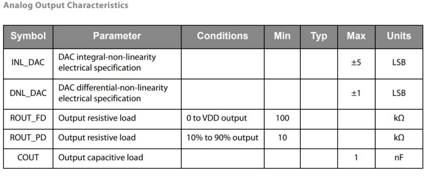
Gerber View
Photos
Video