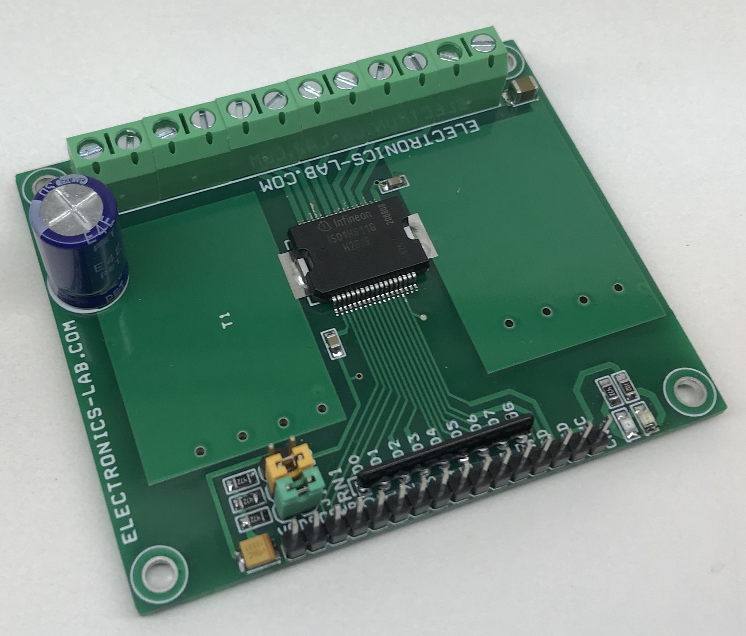
Galvanic Isolated 8 Channel High-Side Switch (0.6A per channel)
This project provides 8 fully protected and isolated high-side power switches that are able to handle current up to 625 mA. An 8-bit parallel microcontroller compatible interface allows connecting the inputs directly to a microcontroller or standalone circuit system.
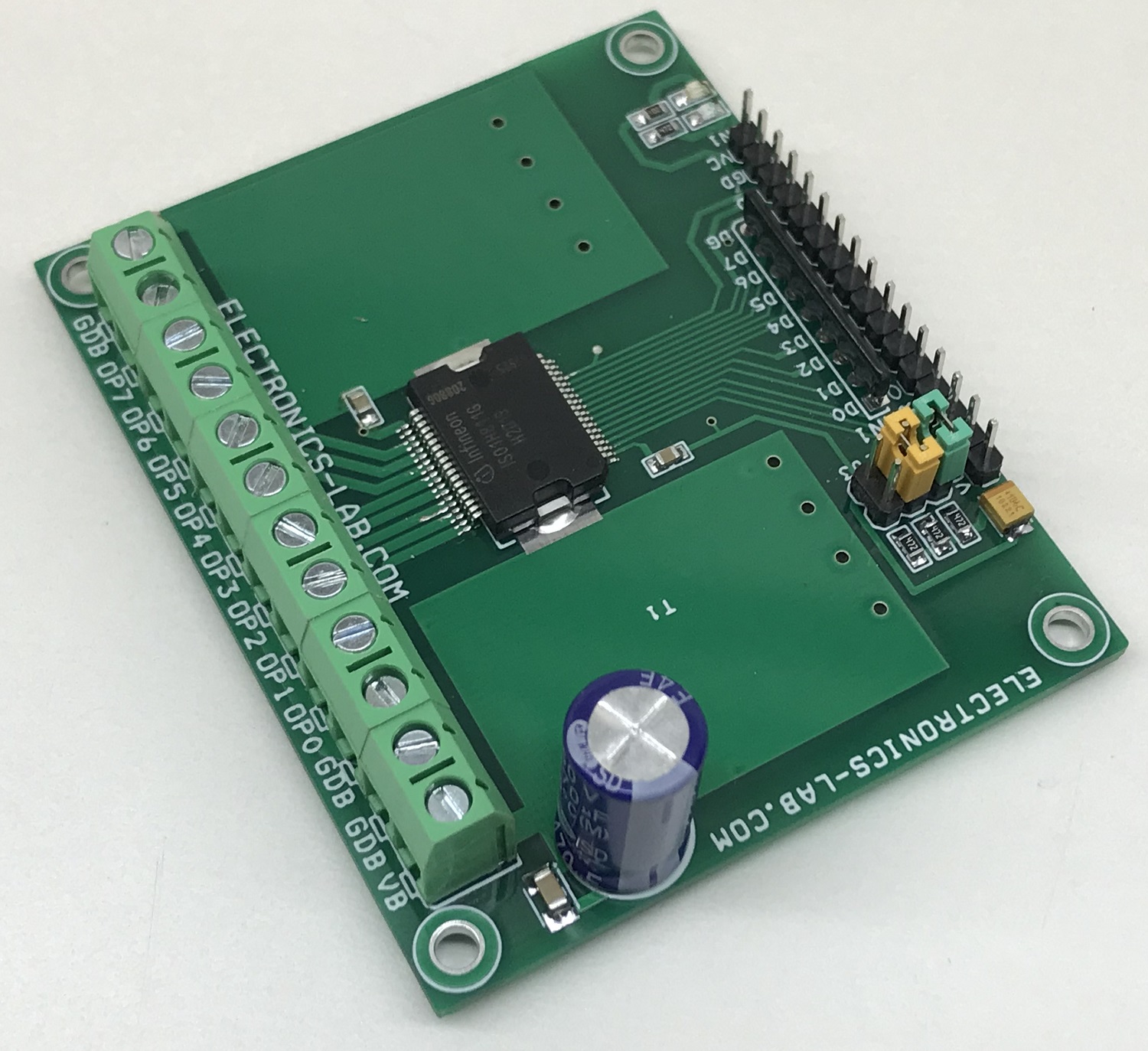
This project provides 8 fully protected and isolated high-side power switches that are able to handle current up to 625 mA. An 8-bit parallel microcontroller compatible interface allows connecting the inputs directly to a microcontroller or standalone circuit system. The input interface also supports direct control mode and is designed to operate with 3.3/5V CMOS compatible levels. The signal transfer from input to output side is realized by the integrated Coreless Transformer Technology. The board is designed for industrial applications such as process control and PLC to drive inductive, resistive, and capacitive loads like Relay, solenoid, lamps, heaters, piezo.
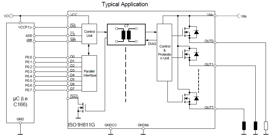
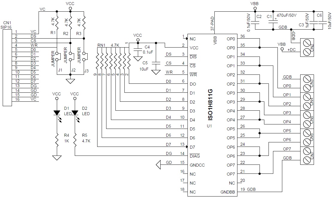
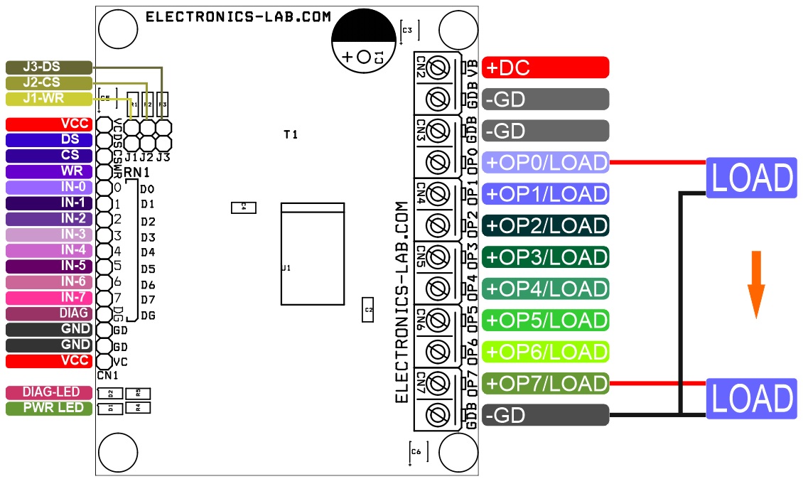
The input can be driven by applying 3.3V/5V CMOS compatible signals to connector CN1. It can operate in microcontroller Mode by using Chip Select and Write Signals or in Direct Control Mode by closing the Jumper J1 and J2 and setting the Data Input from D0 to D7. The Output consists of 8 Channel High Side Switches with 0.6A Current rating. The Output is protected with a channel selected over-temperature switch (to off). The 8 high-side power switches are controlled by means of the integrated parallel interface. The interface is 8-bit μC compatible. Furthermore, a direct control mode can be selected that allows the direct control of the outputs OP0…OP7 by means of the inputs D0…D7 without any additional logic signal. The μC compatible interface allows a direct connection to the ports of a microcontroller without the need for other components. Each of the 8 high-side power switches is protected against short to +DC (VBB), overload, over-temperature, and against over-voltage by an active Zener clamp.
Features
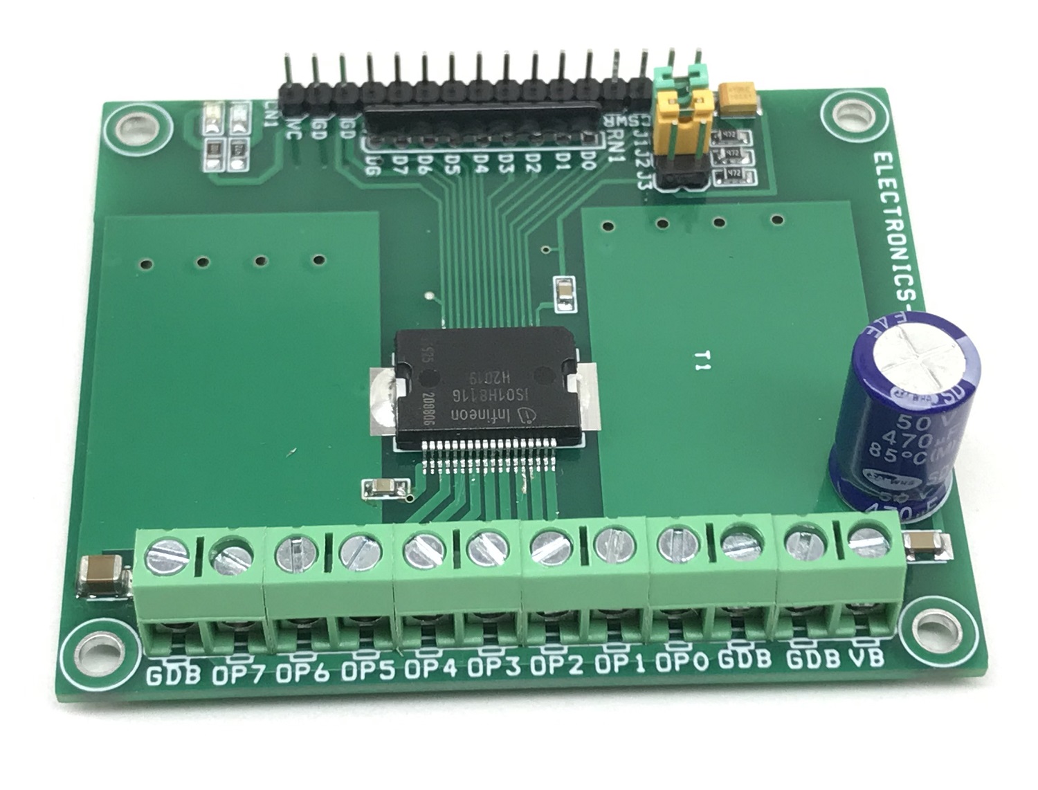
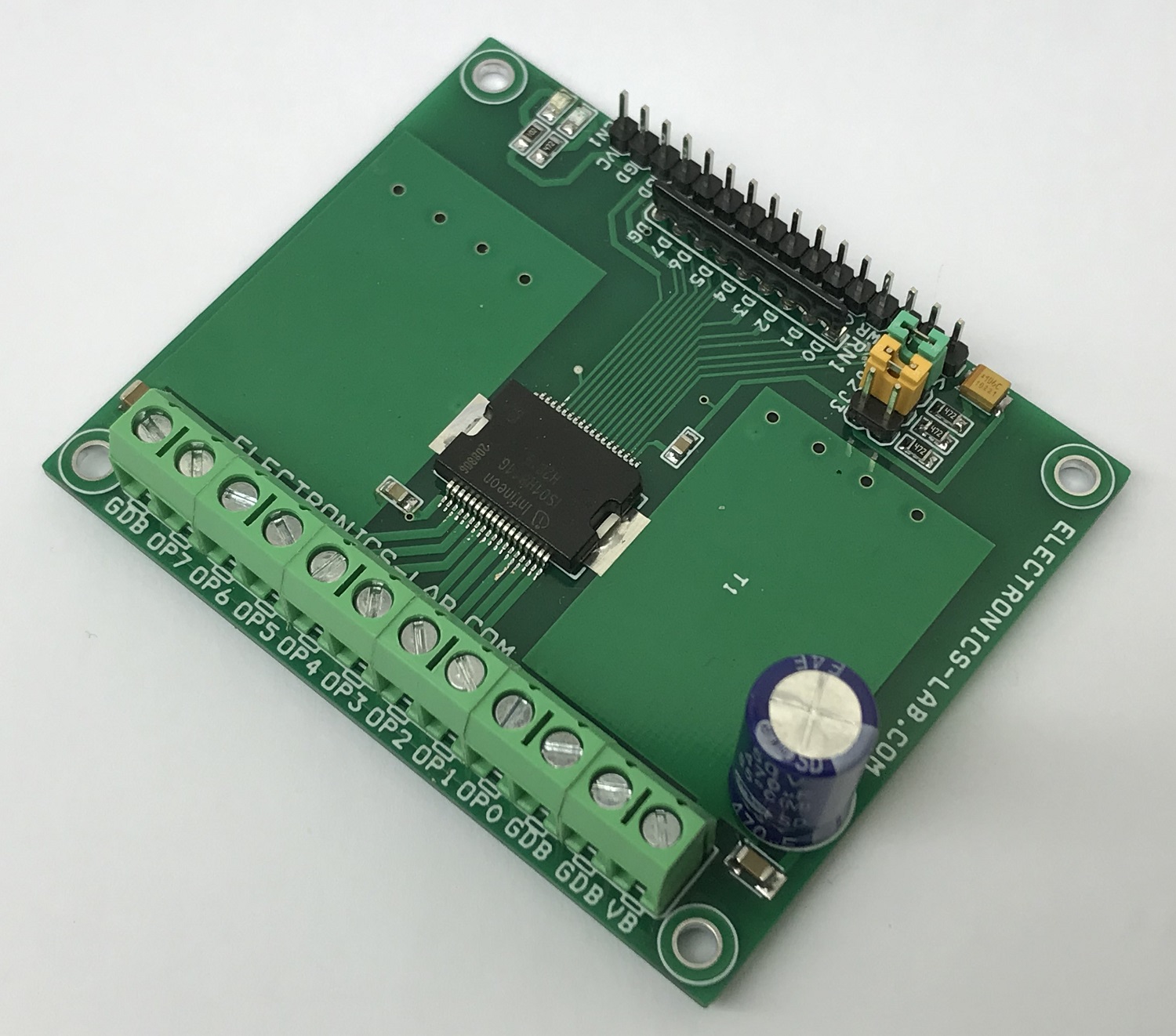
- +DC(VBB) Load Power Supply 11V to 45V (CN2)
- Logic Supply input Side 3.3V to 5V (CN1)
- LED D1 Power LED Logic Supply (Input Side)
- LED D2 LED On When (overtemperature or Vbb (+DC) below ON-Limit is detected)
- Load CN3 to CN7
- Interface 3.3/5V CMOS operation compatible
- Parallel interface
- Direct control mode
- High common-mode transient immunity
- Short circuit protection
- Maximum current internally limited
- Overload protection
- Overvoltage protection (including load dump)
- Undervoltage shutdown with auto-restart and hysteresis
- Switching inductive loads
- Common output disable pin
- Thermal shutdown with restart
- Thermal independence of separate channels
- Common diagnostic output
- ESD protection
- Loss of -GNDBB (GNDbb) and loss of +DC(Vbb) protection
- Reverse Output Voltage protection
- Isolated return path for DIAG signal
- +DC (Vbb) monitoring
- PCB dimensions: 87.49 x 62.07 mm
Testing the Project
Direct mode: CLOSE the Jumper J1, and J2, open the Jumper J3, Connect the Load between OP to GDB, apply load power supply to CN2, apply logic supply to CN1, Output will be default high due to pullup Resister network on input, pull down the input pin D0 by connecting to GND or using micro-controller, the output will be OFF. LED D1 Power LED for logic supply, LED D2 turn ON When overtemperature or Vbb (+DC) below ON-Limit is detected.
Jumper J3 (DIS) DIS (Output disable) Jumper J3 Close = Disable Output, Open Enables the Output
The high-side outputs OUT0…OUT7 can be immediately switched off by means of the low active pin DIS that is an asynchronous signal. The input registers are also reset by the DIS signal. The Output remains switched off after a low-high transition of the DIS signal, till new information is written into the input register. Current Sink to GNDCC.
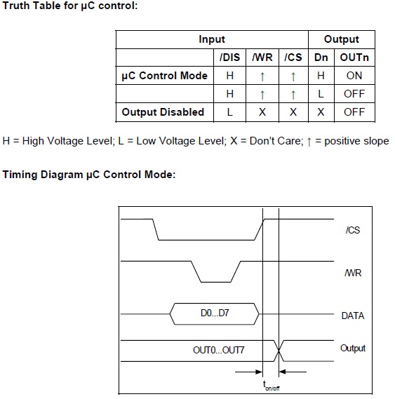
Micro-Controller Mode: μC Control Mode /CS – Chip select. The system microcontroller selects the ISO1H811G by means of the CS pin. Whenever the pin is in a logic low state, data can be transferred from the μC. /WR – Write. The system controller enables the writing procedure in the ISO1H811G by means of the signal WR. A logic low state signal at pin WR writes the input data into the input latches when the CS pin is in a logic low state. D0…D7. The parallel input data is transferred to the input latches with a high-to-low transition of the signal /WR (write) while the /CS is logic low. Then a low-to-high transition of /CS transfers the data of the input latches to the output buffer. The μC Control Mode can be operated by connecting a Processor Board to the corresponding Signals of Connector CN1. Refer to datasheet of the chip to operate in micr0-controller mode.
Schematic
Parts List
| NO. | QNTY. | REF. | DESC | MANUFACTURER | SUPPLIER | SUPPLIER PART NO |
|---|---|---|---|---|---|---|
| 1 | 1 | CN1 | 16 PIN MALE HEADER 2.54MM PITCH | ADAM TECH | DIGIKEY | 2057-PH1-16-UA-ND |
| 2 | 6 | CN2-CN7 | 2 PIN SCREW TERMINAL 5.08MM PITCH | PHOENIX | DIGIKEY | 277-1247-ND |
| 3 | 1 | C1 | 470uF/50V ELECTROLYTIC | PANASONIC | DIGIKEY | P10400TB-ND |
| 4 | 2 | C2,C4 | 0.1uF/50V SMD SIZE 0805 | MURATA/YAGEO | ||
| 5 | 1 | C3 | 1uF/50V SMD SIZE 1206 OR 1210 | MURATA/YAGEO | ||
| 6 | 1 | C5 | 10uF/10V TANTALUM SIZE 1210 OR 1206 | AVX CORPORATION | DIGIKEY | 478-3451-1-ND |
| 7 | 1 | C6 | 10uF/50V SMD SIZE 1210 | MURATA/YAGEO | ||
| 8 | 2 | D1,D2 | LED SMD SIZE 0805 | OSRAM | DIGIKEY | 475-1278-1-ND |
| 9 | 3 | J1,J2,J3 | JUMPER/SHUNT | SULLINS | DIGIKEY | S9001-ND |
| 10 | 4 | R1,R2,R3,R5 | 4.7K 5% SMD 0805 | MURATA/YAGEO | ||
| 11 | 1 | R4 | 1K 5% SMD 0805 | MURATA/YAGEO | ||
| 12 | 1 | U1 | ISO1H811G | INFINION | DIGIKEY | ISO1H811GAUMA1CT-ND |
| 13 | 1 | RN1 | 4.7K RAPCK 9 PIN | BOURNS INC | DIGIKEY | 4309R-101-472LF-ND |
Connections
Truth Table
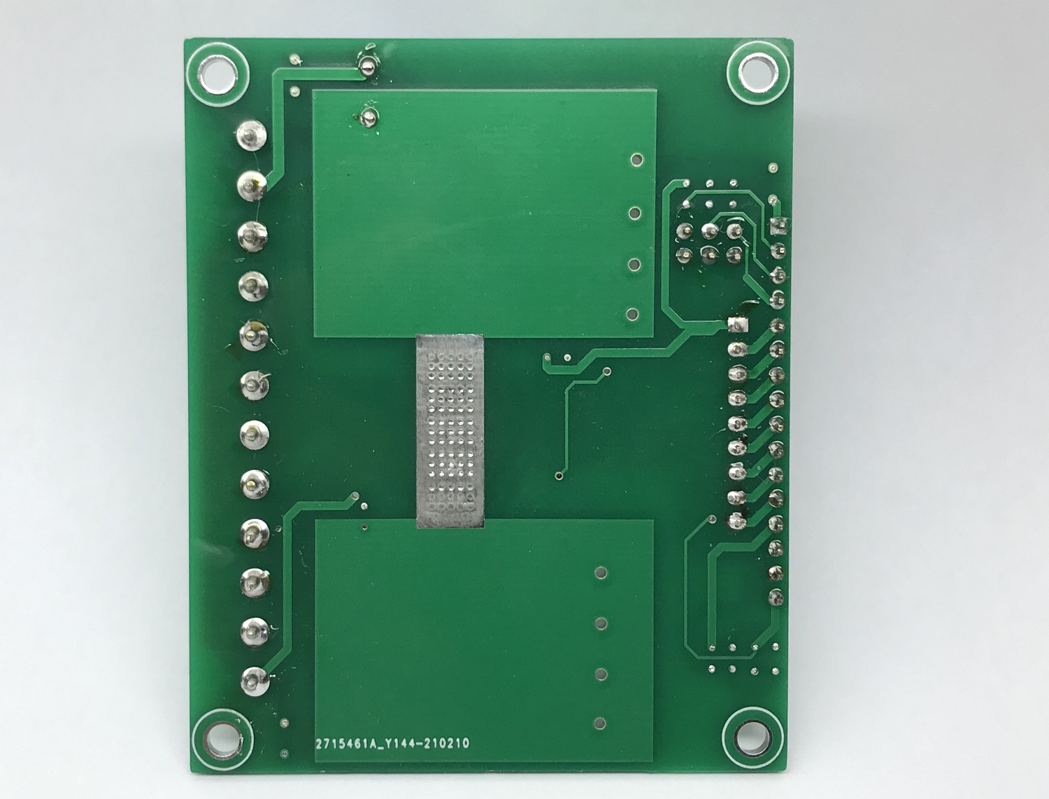
Gerber View
Photos