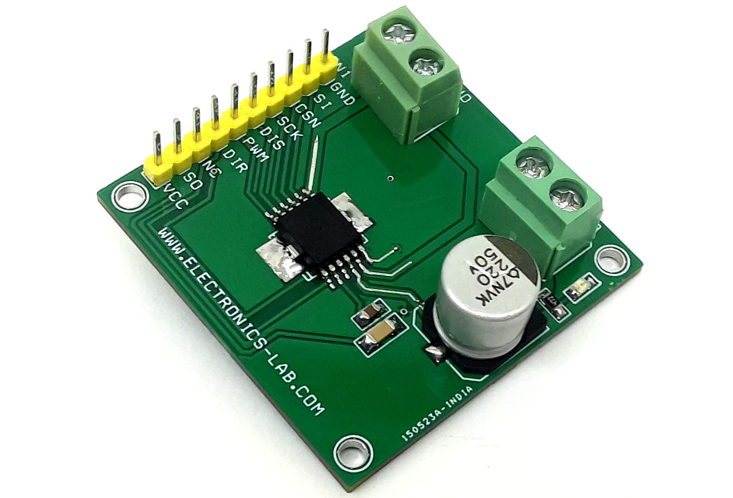
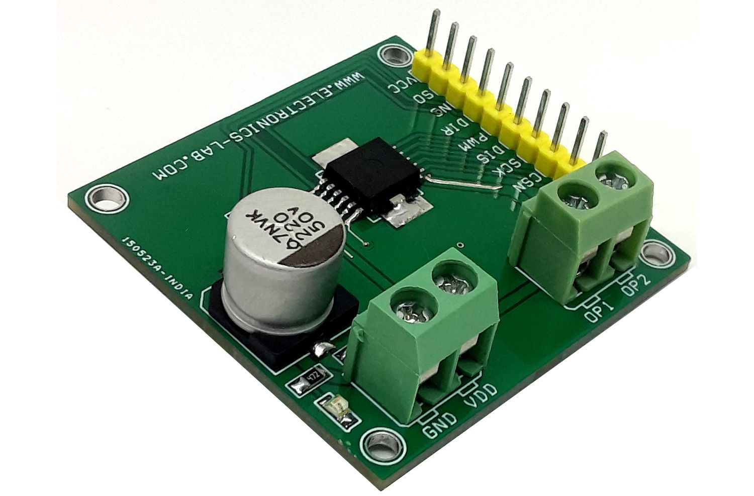
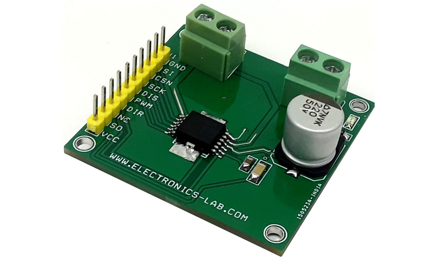
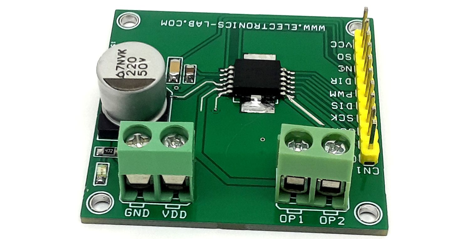
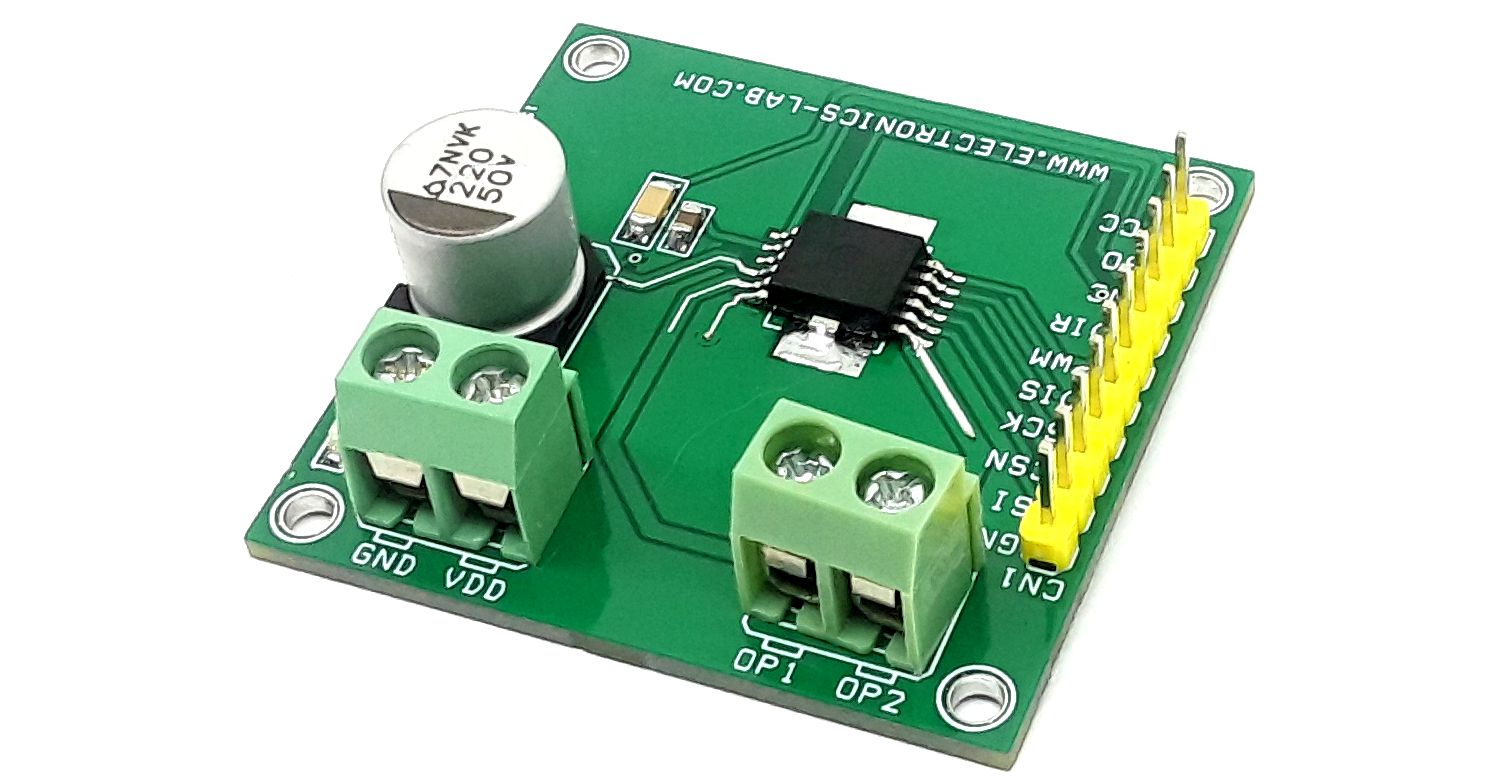
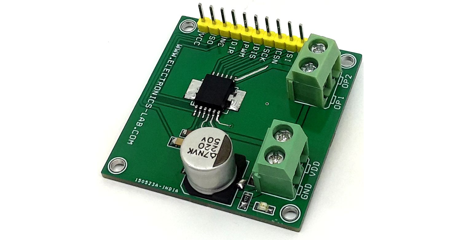
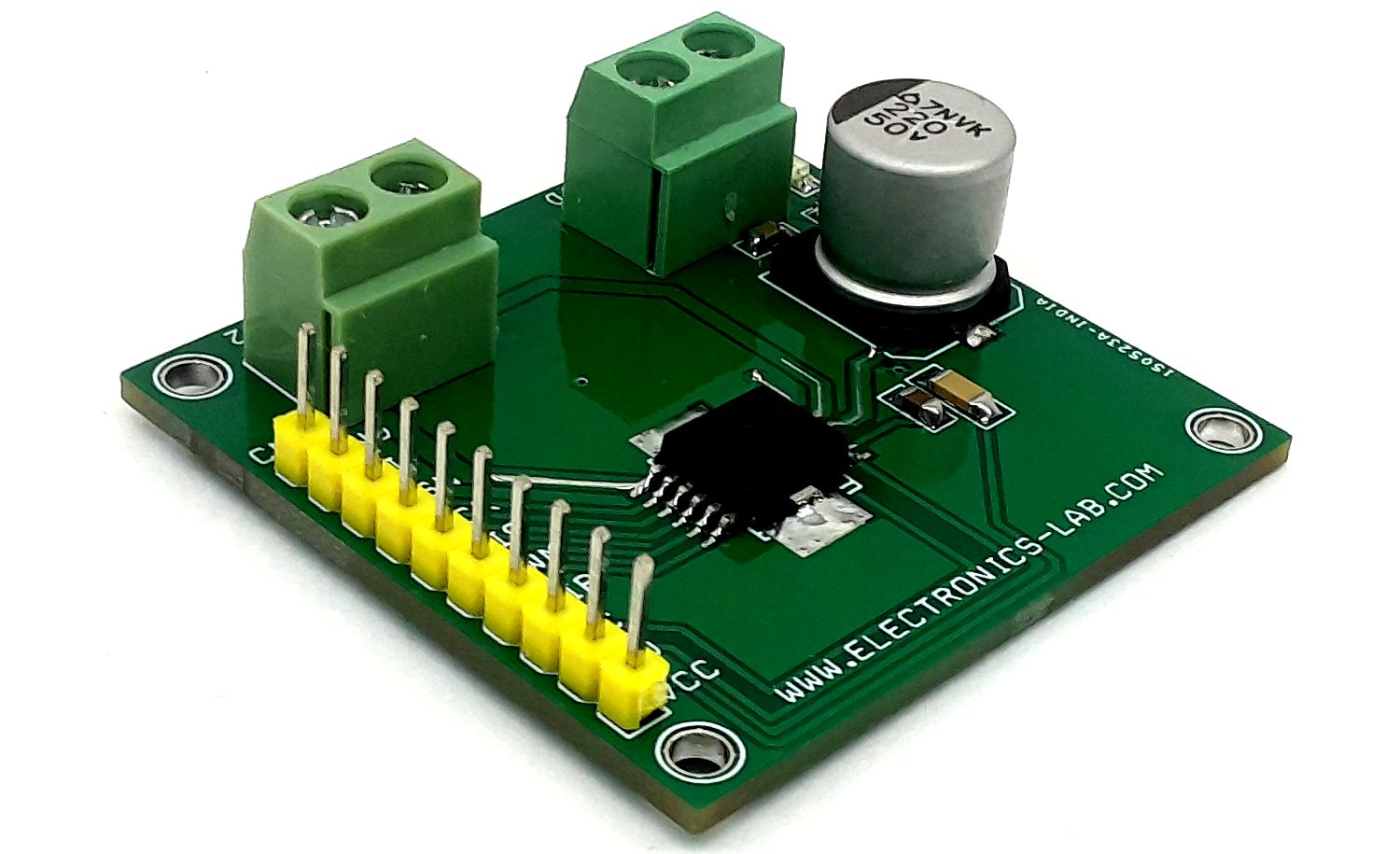
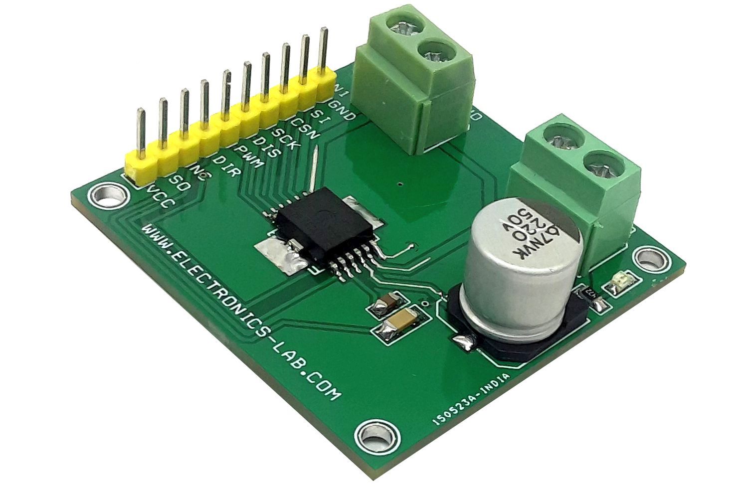
6A H-Bridge with PWM-DIR input and SPI Interface
This 6A H-Bridge is designed for the control of DC motors or other inductive loads. The outputs can be pulse width modulated at frequencies up to 20kHz.
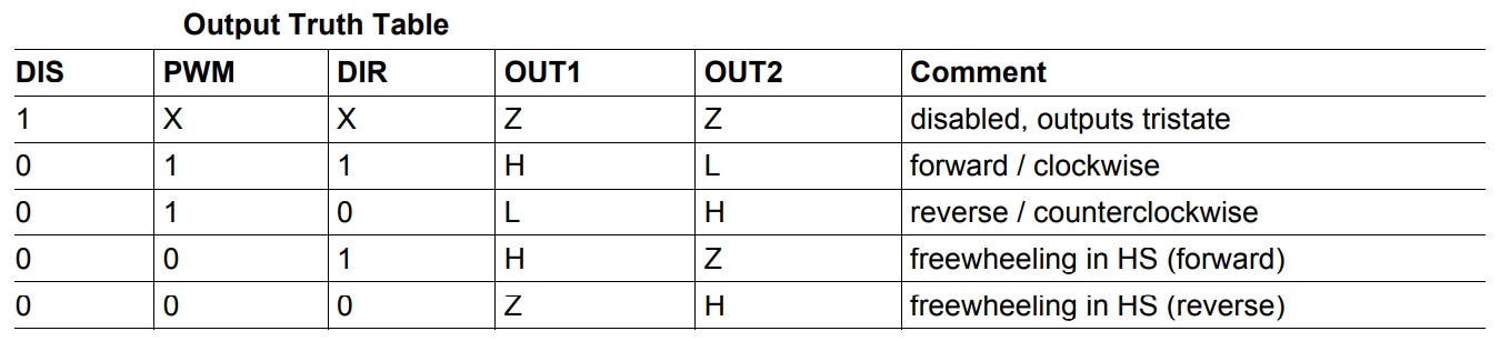
This 6A H-Bridge is designed for the control of DC motors or other inductive loads. The outputs can be pulse width modulated at frequencies up to 20kHz. PWM/DIR control reduces the number of PWM-capable pins needed on the microcontroller side. For load currents above the current limitation threshold (8A typ.) the H-Bridge goes into chopper current limitation mode. It is protected against short circuits and overtemperature and provides extensive diagnosis via SPI or basic feedback via an error flag. An open load can be detected when the bridge is disabled or during the PWM operation of inductive loads. The project is controlled using the inputs PWM and DIR. The signal at DIR is defining the direction of the driven DC motor whereas the PWM signal sets the duty cycle. The outputs can be set tristate (i.e. high side and low side switches are turned off) by setting DIS to high level.
Selecting a DC motor
The board can drive small DC motors with peak currents of up to 6 A. The achievable continuous drive current is lower and depends on supply voltage, switching frequency, and cooling conditions. Realistic continuous drive currents for this project are in the range of 1 A to 2.5 A. Many motors for toys, RC models, or robotics fall in this range.
Features
- Power Supply for the Load 8V to 30V DC (Max 36V)
- RDSon of 100 mΩ per switch typ. at Tj=25 °C
- Logic inputs 3.3 V and 5.0 V TTL/CMOS-compatible
- PWM Frequency up to 20Khz, Duty Cycle 0 to 100%
- PWM and DIR signal 3.3V to 5V Level
- Low standby current
- Chopper current limitation
- Short circuit shut down with latch behavior
- Overtemperature shut down with latch behavior
- VS undervoltage shutdown
- Open load detection in ON and OFF state
- Detailed SPI diagnosis or simple error flag
- PCB Dimensions 43.18 x 41.91 mm
- 4 x 2.5 mm Mounting Holes
Protection and Diagnostics; Both output stages of the IFX9201SG are equipped with fault diagnostic functions:
- Short-to-supply voltage (SCVS)
- Short to ground (SCG)
- Open load (OL)
- Over-temperature (OT)
Current Limitation
To limit the output, current a chopper current limitation is integrated. Current measurement for current limitation is done in the high side path. When the current in high-side switch of OUT1 (HS1) exceeds the limit IL longer than the blanking time tb, the low side switch of OUT2 (LS2) is switched off, independent of the input signal at PWM. This leads to freewheeling through the bulk diode of HS2 and therefore to a decrease of the load current. As soon as the current falls below IL, OUT2 is switched back to normal operation, i.e. the outputs follow the inputs according to the truth table. To avoid high switching frequencies in case of low inductive loads the minimum time between two transitions is limited to t-trans.
The short circuit to ground detection is activated when the current through one of the high side switches rises over the threshold ISC and remains higher than ISC for at least the filter time tsdf within the blanking time tb. Both outputs will be switched off and the failure will be reported in the SPI diagnosis register. The outputs can be re-activated by disabling and enabling the bridge via the disable signal DIS, pulling VSO to GND or by a reset command via SPI
Serial Peripheral Interface (SPI)
For diagnosis purposes, the IFX9201SG is equipped with a “Serial Peripheral Interface “(SPI). The SPI of several IFX9201SGs can be connected in daisy chain configuration in order to save microcontroller interface pins. The IFX9201SG is configured as a “slave” device. This means that the µC as the master is providing the chip select (CSN) and the clock signal (SCK). A data transfer on the SPI bus is initiated with a falling edge on CSN and is terminated by a rising edge on CSN.
The data on the serial input pin SI is sampled with the falling edge of SCK, and the serial data output at SO is determined by the rising clock edge. The data is transferred “MSB first”. The word length of the SPI is 8 bit. Please note that there is no check for the number of clocks within a SPI frame. Any low pulse at CSN will be regarded as one frame
Short Circuit to Supply
A short circuit to the supply voltage VS is detected in the same way as a short circuit to ground, only in the low side switch instead of the high side switch.
Short Circuit over Load
Short circuit overload will trigger the short circuit detection either of the high side or the low side switch (whichever is faster).
Overtemperature
In case of high DC currents, insufficient cooling, or high ambient temperature, the chip temperature may rise above the thermal shut-down temperature TjSD. In that case, all output transistors are turned off. Overtemperature shutdown is latching. The outputs can be re-activated as soon as the junction temperature has fallen below the switch-on temperature TjSO.
Undervoltage Shut-Down
If the supply voltage at the VS pins falls below the undervoltage detection threshold VUV_OFF, the outputs are turned off. The undervoltage detection is not latching. That means that as soon as VS rises above VUV_ON again, the device is returning to normal operation.
Open Load Detection in OFF state
When the bridge is disabled (DIS=high) the open load in OFF detection becomes active. Two diagnostic current sources will then be connected to the outputs, a pull up current source at OUT1 and a pull-down current source at OUT2. The pull-down current source is stronger than the pull up current source and therefore will pull down OUT1 if a load is present. If no load is present OUT1 will be pulled high by the pull up current source. This is detected by a comparator and reported in the SPI diagnosis register. Please note that capacitors placed at the outputs for EMC reasons first have to be discharged by
the pull-down current source at OUT2 for the open load detection to work properly. Also, if current is flowing through the load at the time of disabling the freewheeling current will force the outputs towards supply voltage VS. This may lead to an erroneous reporting of open load. Therefore, the first diagnostic reading after disabling should be discarded and a second reading should be taken after the load is deenergized and the output capacitors are discharged completely. The open load detection can be disabled by setting the OLDIS bit in the CTRL_REG register. This will disconnect the diagnostic current sources and suppress the reporting of open load in the DIA_REG register
Sleep Mode
In order to minimize current consumption during inactive phases the device can be put into sleep mode by pulling the VSO pin to GND. This functionality can also be used to provide a second switch off path for the outputs similar to an enable pin, simply by driving VSO directly from a microcontroller output. Since VSO is supplying also the output buffer of the SO signal it has to be ensured that the microcontroller output can provide sufficient current.
Please note that the push-pull stage of the SO output provides a current return path to VSO via the bulk diode of the high side MOSFET. Therefore, it has to be ensured that the voltage at SO never exceeds the voltage at VSO by more than 0.3V.
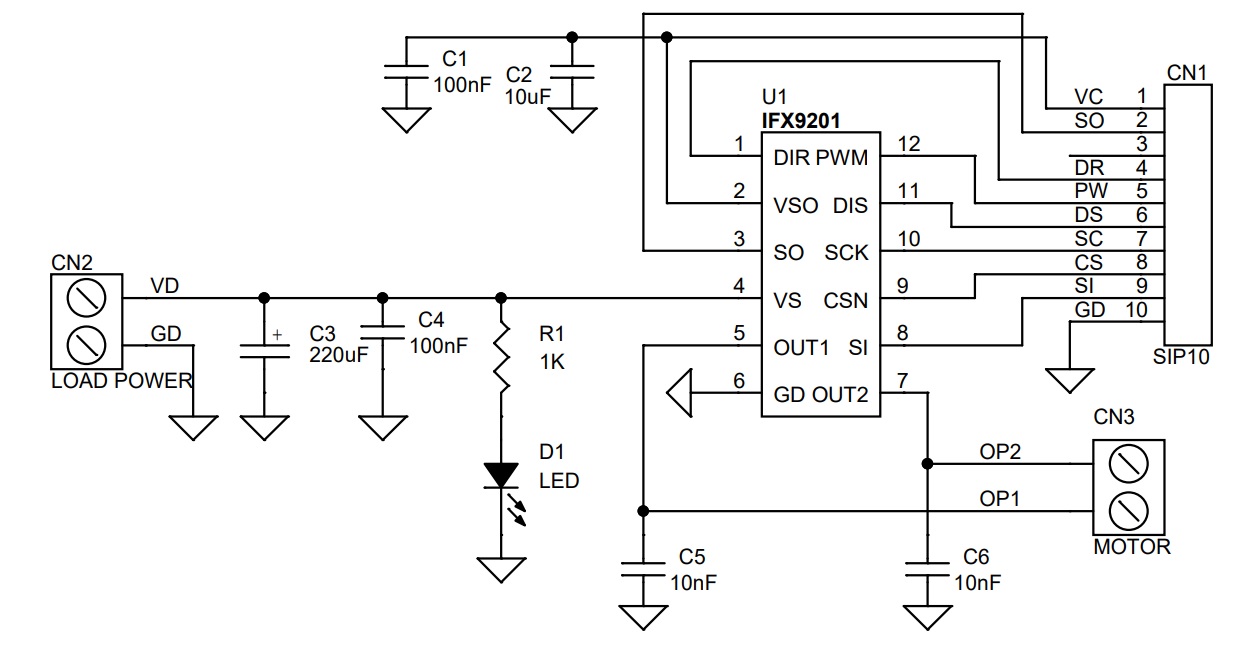
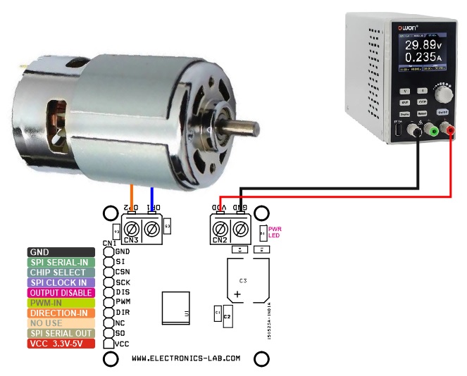
Connections CN1
- Pin 1 VCC 3.3V-5V
- Pin 2 SO SPI Serial Output
- Pin 3 NC (Not Connected)
- Pin 4 Direction Control Input
- Pin 5 PWM Input (For Motor Speed Control), Frequency up to 20Khz, PWM Duty Cycle 0 to 100%
- Pin 6 Disable (Disable the Outputs)
- Pin 7 SPI Clock Input
- Pin 8 SPI Chip Select
- Pin 9 SPI Serial In
CN2: Pin 1 = Load Power Supply Input 8V to 30V DC, Pin 2 = GND
CN3: Pin 1 = Output 1, Pin 2 = Output 2 (DC Motor Connection)
D1: Power LED
Schematic
Parts List
| NO | QNTY. | REF. | DESC. | MANUFACTURER | SUPPLIER | PART NO |
|---|---|---|---|---|---|---|
| 1 | 1 | CN1 | 10 PIN MALE HEADER PITCH 2.54MM | WURTH | DIGIKEY | 732-2670-ND |
| 2 | 1 | CN2 | 2 PIN SCREW TERMINAL PITCH 5.08MM | PHOENIX | DIGIKEY | 277-1247-ND |
| 3 | 1 | CN3 | 2 PIN SCREW TERMINAL PITCH 5.08MM | PHOENIX | DIGIKEY | 277-1247-ND |
| 4 | 2 | C1,C4 | 100nF/50V CERAMIC SMD SIZE 0805 | YAGEO/MURATA | DIGIKEY | |
| 5 | 1 | C2 | 10uF/10V CERAMIC SMD SIZE 1206 | YAGEO/MURATA | DIGIKEY | |
| 6 | 1 | C3 | 220uF/50V ELECTROLYTIC | RUBYCON | DIGIKEY | 1189-1654-1-ND |
| 7 | 2 | C5,C6 | 10nF/50V CERAMIC SMD SIZE 0805 | YAGEO/MURATA | DIGIKEY | |
| 8 | 1 | D1 | LED RED SMD 0805 | LITE ON INC | DIGIKEY | 160-1427-1-ND |
| 9 | 1 | R1 | 1K 5% SMD SIZE 0805 | YAGEO/MURATA | DIGIKEY | |
| 10 | 1 | U1 | IFX9201 | INFINEON | DIGIKEY | IFX9201SGAUMA1CT-ND |
Connections
Truth Table
Gerber View
Photos