

Dual Adjustable Power Supply
- Rajkumar Sharma
- 50.537 Views
- medium
- Tested
- SKU: EL35962
- Quote Now
- 0 Likes

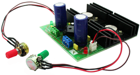
This project is a solution to power up most of devices or projects requiring dual (+/-) adjustable power supply.
Description
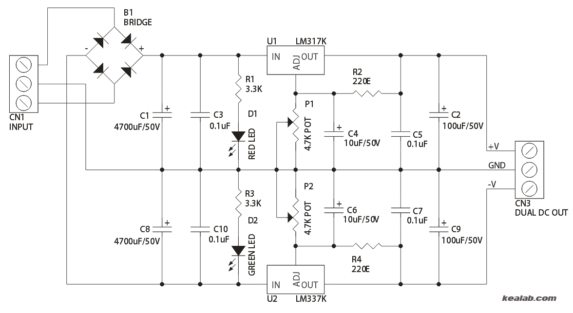
The circuit is based on LM317 positive and LM337 negative voltage regulators. LM317 series of adjustable 3 terminal regulator is capable of supplying in excess of 1.5A over a 1.2V to 30V DC output range, due to TO3 package of IC and large heat sink the power supply can handle maximum load current.
- Output: +/- 1.2 to 30V DC
- Output Current: 1.5Amps
- Supply Input: 24V-0-24V AC, 2Amps Center tape Transformer
- CN1: Transformer Connections
- CN3: +/- Dual Supply Outputs
- P1: Positive Voltage Adjust
- P2: Negative Voltage Adjust
- D1: Positive Power Indicator
- D2: Negative Power Indicator
Schematic
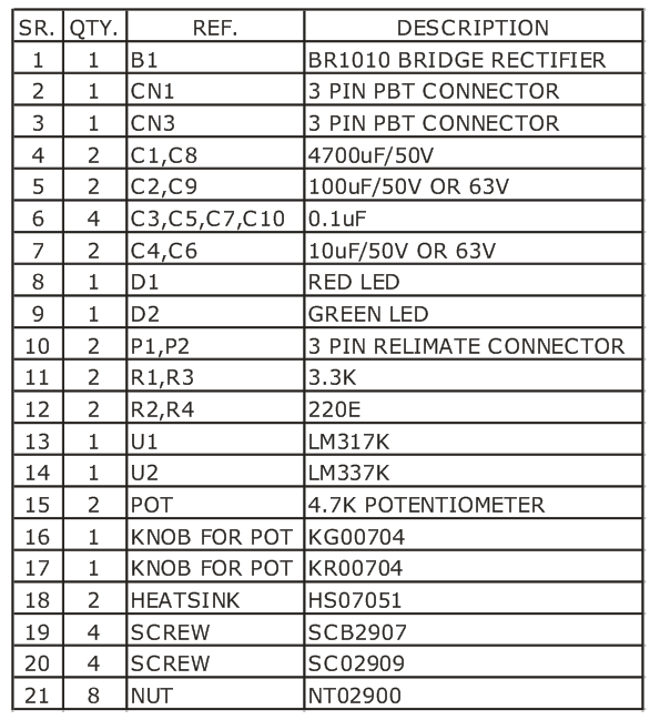
Parts List
Please follow and like us:
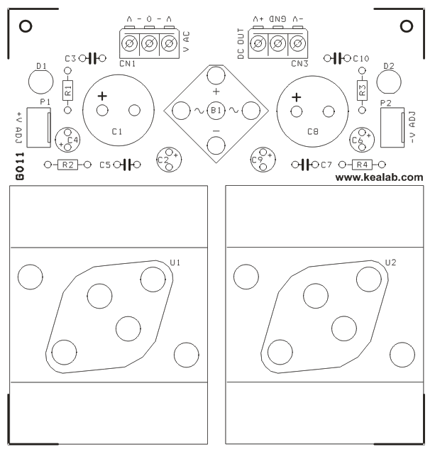
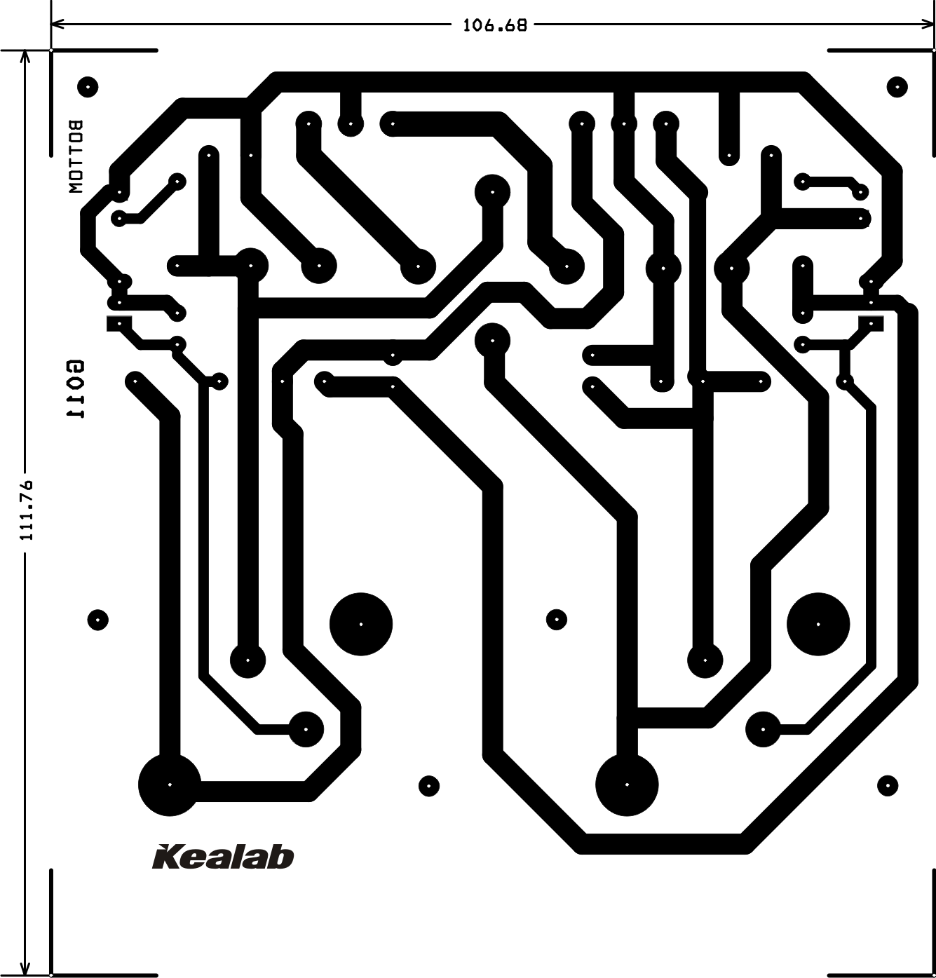
PCB


can the transformer be replaced with a higher current rating like 3 or 5 amps?
Sure, it will not be a problem to use a higher rating transformer if the voltage is still 24V
Can I use this two 220VAC/12VAC halogen transformer serial connected?
http://www.ebay.es/itm/201209984483?_trksid=p2060353.m1438.l2649&var=500403606005&ssPageName=STRK%3AMEBIDX%3AIT
If they have 12VAC 60W output each, I should get 24VAC 120W 5A output.
Or this one :
http://www.ebay.es/itm/361038813028?_trksid=p2060353.m1438.l2649&var=630376295270&ssPageName=STRK%3AMEBIDX%3AIT
Connected directly to the output of the diode bridge.
Which one is the best option?
Thanks
How can I make the output voltage be 0-30 volts?
thankyou
Very good work
what would be the output voltage range if i only used a 15 – 0 – 15 transformer? thank you. great work by the way, neat and nice.
With a 15Vac transformer you will get around 21V peak voltage, minus the voltage drop in rectifier and regulator you will get around 16-17V at the output.
Please I need to implement this as a 12V, 2A dual output unit what modifications do I need to make.
LM317 can go up to 2.2A, so you can try with a bigger transformer to get that current output.
why not LM317T or LM337T ?
I used 24-0-24V, 1Amp Transformer as i needed max 1 Amp. The problem with the circuit is, without any load connected o/p is 1.5V to ~33V at positive side and the same with negative side ( obviously with -ve values). (after measuring on multi-meter) But, as i connect any load the +ve side provides stable and proper voltage supply. However, on -ve side it just stuck around 1.5V to 3V. I checked for any short circuits, bypass capacitors, etc. And every thing is seems good. But, only at pin’s of LM337 might be problem . so, i tried with LM905 and the same thing happens with it. no voltage at output when load is connected.
Please, let me know what’s happening? and how to make corrections?
Thanks in Advance…
What load do you connect? How much current it draws?
What is 220E?
It’s 220 Ohm
Can i change the bridge rectifier into 4 silicon diode (1N4007)?
No, you will need diodes that can withstand higher currents, at least 3A to be on the safe side.
please add pcb layout in pdf format
PCB in PDF is attached above. Thanks
why the starting voltage is 1.2v ? how can i get 0 volts in the start ?
Because LM317/337 need reference voltage of 1.25V.
It’s possible to go to zero but the design need to change.
Hi, I just made this circuit but I’m having problem in the – ve voltage section. The positive voltage can be regulated but the negative side voltage has no impact
Could you open a community topic and post more info on the transformer you use and the connections? This is the best place to get help about your project.