

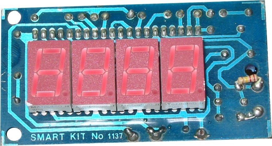
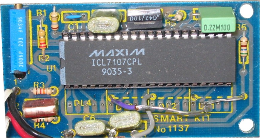
Led display digital Voltmeter
- http://www.smartkit.gr
- 134.404 Views
- medium
- Tested
- 0 Likes

Copyright of this circuit belongs to Smart kit electronics. On this page, we will use this circuit to discuss improvements and we will introduce some changes based on the original schematic.
General Description
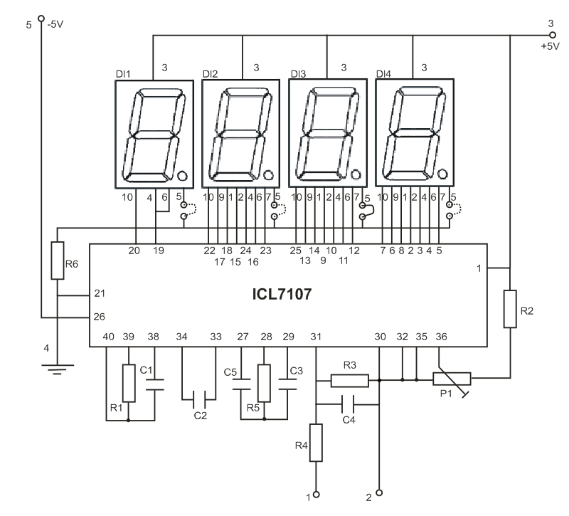
This is easy to build, but nevertheless very accurate and useful digital voltmeter. It has been designed as a panel meter and can be used in DC power supplies or anywhere else it is necessary to have an accurate indication of the voltage present. The circuit employs the ADC (Analogue to Digital Converter) I.C. CL7107 made by INTERSIL. This IC incorporates in a 40 pin case all the circuitry necessary to convert an analog signal to digital and can drive a series of four seven-segment LED displays directly. The circuits built into the IC are an analog to digital converter, a comparator, a clock, a decoder, and a seven-segment LED display driver. The circuit as it is described here can display any DC voltage in the range of 0-1999 Volts.
Technical Specifications – Characteristics
- Supply Voltage: …………. +/- 5 V (Symmetrical)
- Power requirements: ….. 200 mA (maximum)
- Measuring range: ………. +/- 0-1,999 VDC in four ranges
- Accuracy: ………………….. 0.1 %
Features
- Small size
- Easy construction
- Low cost.
- Simple adjustment.
- Easy to read from a distance.
- Few external components.
How it Works
In order to understand the principle of operation of the circuit, it is necessary to explain how the ADC IC works. This IC has the following very important features:
- Great accuracy.
- It is not affected by noise.
- No need for a sample and hold circuit.
- It has a built-in clock.
- It has no need for high accuracy external components.
An Analogue to Digital Converter, (ADC from now on) is better known as a dual-slope converter or integrating converter. This type of converter is generally preferred over other types as it offers accuracy, simplicity in design, and relative indifference to noise which makes it very reliable. The operation of the circuit is better understood if it is described in two stages. During the first stage and for a given period the input voltage is integrated, and in the output of the integrator at the end of this period, there is a voltage that is directly proportional to the input voltage. At the end of the preset period, the integrator is fed with an internal reference voltage and the output of the circuit is gradually reduced until it reaches the level of the zero reference voltage. This second phase is known as the negative slope period and its duration depends on the output of the integrator in the first period. As the duration of the first operation is fixed and the length of the second is variable it is possible to compare the two this way the input voltage is in fact compared to the internal reference voltage and the result is coded and is sent to the display.
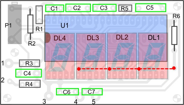
All this sounds quite easy but it is in fact a series of very complex operations which are all made by the ADC IC with the help of a few external components which are used to configure the circuit for the job. In detail the circuit works as follows. The voltage to be measured is applied across points 1 and 2 of the circuit and through the circuit R3, R4 and C4 is finally applied to pins 30 and 31 of the IC. These are the input of the IC as you can see from its diagram. (IN HIGH & IN LOW respectively). The resistor R1 together with C1 are used to set the frequency of the internal oscillator (clock) which is set at about 48 Hz. At this clock rate there are about three different readings per second. The capacitor C2 which is connected between pins 33 and 34 of the IC has been selected to compensate for the error caused by the internal reference voltage and also keeps the display steady. The capacitor C3 and the resistor R5 are together the circuit that does the integration of the input voltage and at the same time prevent any division of the input voltage making the circuit faster and more reliable as the possibility of error is greatly reduced. The capacitor C5 forces the instrument to display zero when there is no voltage at its input. The resistor R2 together with P1 are used to adjust the instrument during set-up so that it displays zero when the input is zero. The resistor R6 controls the current that is allowed to flow through the displays so that there is sufficient brightness with out damaging them. The IC as we have already mentioned above is capable to drive four common anode LED displays. The three rightmost displays are connected so that they can display all the numbers from 0 to 9 while the first from the left can only display the number 1 and when the voltage is negative the «-« sign. The whole circuit operates from a symmetrical ρ 5 VDC supply which is applied at pins 1 (+5 V), 21 (0 V) and 26 (-5 V) of the IC.
Parts List
R1 = 180k
R2 = 22k
R3 = 12k
R4 = 1M
R5 = 470k
R6 = 560 Ohm
C1 = 100pF
C2, C6, C7 = 100nF
C3 = 47nF
C4 = 10nF
C5 = 220nF
P1 = 20k trimmer multi turn
U1 = ICL 7107
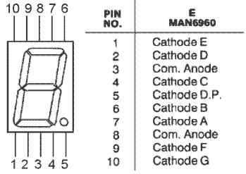
LD1,2,3,4 = MAN 6960 common anode led displays
0-20 V ….R3 = 1.2K
0-200 V …R3 = 12K
0-2000 V ..R3 = 120K
Construction
First of all let us consider a few basics in building electronic circuits on a printed circuit board. The board is made of a thin insulating material clad with a thin layer of conductive copper that is shaped in such a way as to form the necessary conductors between the various components of the circuit. The use of a properly designed printed circuit board is very desirable as it speeds construction up considerably and reduces the possibility of making errors. To protect the board during storage from oxidation and assure it gets to you in perfect condition the copper is tinned during manufacturing and covered with a special varnish that protects it from getting oxidised and also makes soldering easier.
Soldering the components to the board is the only way to build your circuit and from the way you do it depends greatly your success or failure. This work is not very difficult and if you stick to a few rules you should have no problems. The soldering iron that you use must be light and its power should not exceed the 25 Watts. The tip should be fine and must be kept clean at all times. For this purpose come very handy specially made sponges that are kept wet and from time to time you can wipe the hot tip on them to remove all the residues that tend to accumulate on it.
DO NOT file or sandpaper a dirty or worn out tip. If the tip cannot be cleaned, replace it. There are many different types of solder in the market and you should choose a good quality one that contains the necessary flux in its core, to assure a perfect joint every time.
DO NOT use soldering flux apart from that which is already included in your solder. Too much flux can cause many problems and is one of the main causes of circuit malfunction. If nevertheless you have to use extra flux, as it is the case when you have to tin copper wires, clean it very thoroughly after you finish your work.
In order to solder a component correctly you should do the following:
- Clean the component leads with a small piece of emery paper.
- Bend them at the correct distance from the component’s body and insert the component in its place on the board.
- You may find sometimes a component with heavier gauge leads than usual, that are too thick to enter in the holes of the p.c. board. In this case use a mini drill to enlarge the holes slightly.
- Do not make the holes too large as this is going to make soldering difficult afterwards.
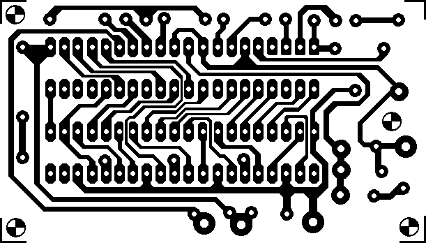
PCB


 Converter")

")
please give me the details of components
Parts list added above. Thanks for letting me know
where & how much i/p voltage can feed & which are i/p terminals….
Input voltage is applied to pin 1 and 2 and can be up to 2kV when R3=120kOhm
how R1=180K and C1=100pf sets frequency 48 Hz as given above ???? and what is relation of frequency with number of readings per second???
It is written that R1 and C1 se the frequency to 48hz but it is wrong. I have gone through tha data sheet of ic there is 48k hz.
hi.tnx for good information.
thanks alot man ! great work keep it up !
are the 26th ic terminal and 21st ic terminal connected with resistor r6 or -5 voltage 26th terminal is alone
in the given circuit what is “P1”?????????????
Its the trimmer potentiometer for calibration ! the little blue thing in the corner
its a 20k trimming potentiometer
How would you supply -5v to the IC?
You will need a power supply like this: https://www.electronics-lab.com/project/5v-symmetrical-regulated-power-supply/
Is it necessary to use this power supply,can’t we use 9v battery and LM7805 as a Power Supply Circuit and connect the -V pin to ground?
Yes, you can power this LED Display Voltmeter using a single power source.
is that the pcb actual size?
To find out the correct PCB dimensions you have to print it some times at different scales and try to fit the IC on the print.
Try using DIPTrace for designing the PCB it has hundreds of default footprints of components.
c6??????c7?????
C7 and C6 are 100nF filter capacitors not shown in schematic
Admin i build this project together with your ct power supply but i have a little problem. my project is 1.5v output but the meter is continues moving in from 1.2 to 4.5v over and over again.
therefore i can’t point the voltage bcause of continuous voltage varying. may ps is min of 1.5v and 24v max. what parts can i replace to prevent for moving the meter.
Please double check connections and input voltage ripple. You may also add a bigger filter cap.
Can the wise men in electronics guide me to any schematic, showing how to connect this display(or any other) to a zero to 30 v current limiting power supply I built recently. Will be very grateful. Do not have much experience. Thanks Electronics Lab.
i have i digital volt meter but when voltage is high it show correct value but voltage is low it show 185–190 volt but in actual voltage is 155-175 what should i do when part should i cahnge
Try to adjust P1 when there is no voltage input so it displays zero on 7-segment displays.
hi need measure 300 vdc how can i change the range
You will need to add an additional voltage divider to scale the 300Vdc to 2Vdc and be sure to use high value resistors to limit the current consumption on the resistor divider.
hey this circuit in breadboard always shows 666 ..so please give me the solution
Please double check your connections and part alignment.
in the copper side of this project stated above in first image have 1 resistor 120k connected in pin 1 in the same time the copper clad is connected. what is the purpose and function of resistor in connected to pin 1?
Hi, I have assembled all the parts as per the diagram. However, the unit display constantly displays random numbers. When the circuit is connected to a power source, the display is unstable. Can anyone help me please ?
Sir is it necessary to use MAN6960 led display or I can use any common anode single digit display
You can use any common anode display.
it displays the maximum value of 199.9 continuously and there is no change when inputs are given.`please i need the reply fast
istead of supply -5 can we common it..
On some applications negative supply can be omitted. For more information on negative supply please read page 10 of ICL7107 datasheet (chapter “ICL7107 Power Supplies”) Datasheet here: http://www.intersil.com/content/dam/Intersil/documents/icl7/icl7106-07-07s.pdf
I am confusing about the supply voltage for this project. Is it +5 -5 volt and zero ground?
You are right, this circuit uses +5V, -5V referred to GND. So you need a symmetrical power supply like the one here: https://www.electronics-lab.com/project/5v-symmetrical-regulated-power-supply/
At point 1&2 voltage should be ac or dc & what is i/p voltage at point 1&2,pl tell me.
The voltage at pins 1-2 is DC only.
can i use icl 7117 instead of 7107? If yes, what changes should I apply?
Yes, you can use ICL7117. The difference with 7107 is that 7117 has a hold pin to enable LED display freeze function.
Hi
I would like to measure the output voltage in mV range, and my input voltage will be given by the Piezoelectric diodes (pressure sensor). Will this board will work to measure the voltage out of it?
On the datasheet page 4 you can see the configuration for 200mV full scale. https://www.intersil.com/content/dam/Intersil/documents/icl7/icl7106-07-07s.pdf So it should measure down to few mV
Can I measure AC voltage with this, pls help
This is discussed here: https://electronics-lab.com/community/index.php?/topic/41509-digital-ac-voltmeter-using-7107/
What is the maximum voltage it can measure?
The circuit as it is described here can display any DC voltage in the range of 0-1999 Volts.
I measured the voltage -48V but the display is not stable